

Continuing our look at the IMAPS Onshoring conference with a look at U.S. OSAT activities.
(We should note that while this conference was listed for US & Canadian Citizens only, we are showing materials that were explicitly listed as “Unclassified; approved for public release; distribution unlimited” only.)
IBM Bromont
Rox Lemire of IBM Bromont offered that advanced packaging required:
- Confidence in partnership
- Often needs custom strategies with required client / OSAT co-development
- Scalable options for this are limited in N.A.
Bromont believes that a full-service OSAT offers:
- Less exposure to your sensitive data (IP)
- Easier parallel development work
- Smoother integration toward production
- One focal point for your project
IBM Bromont background:
- 50 years of packaging manufacturing experience serving both IBM and external customers with advanced flip ship, SiP, and photonic assembly and test.
- Supports IBM products including high-end systems such as Z series and Power series.
- Is a certified US trusted foundry for packaging of US classified parts
- Has the capability and capacity to support packaging for DoD and commercial customers
- Massive expansion is planned in both capability and capacity supported by Canadian Government funding.
Bromont current capabilities include:
- Development and prototyping
- High-volume manufacturing (HVM)
- Dice sort and pick (DSP)
- Test: wafer, module, SLT, burn-In
- Reliability (JEDEC and beyond)
- Bond and assembly
- Flip chip of any die size
- Laminate from 13 x 13mm to > 100 x 100mm
- Build up layers up to 9-2-9
- Thermal management > 500W
- HI and HDI (up to 40um pitch)
- CSP, 2.3D, silicon bridge (DBHi)
- Prototype 2.5D and 3D
- SiP with > 400 components in production
- Opto-electronics
INTEGRA
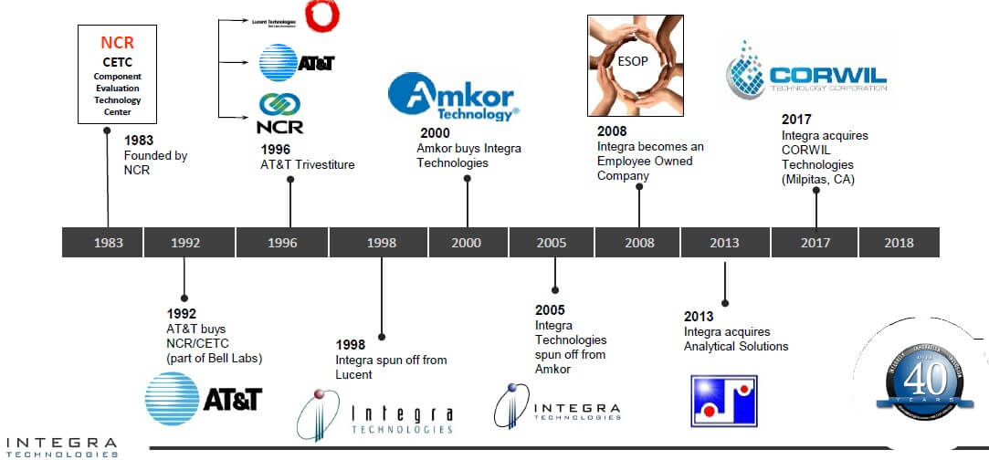
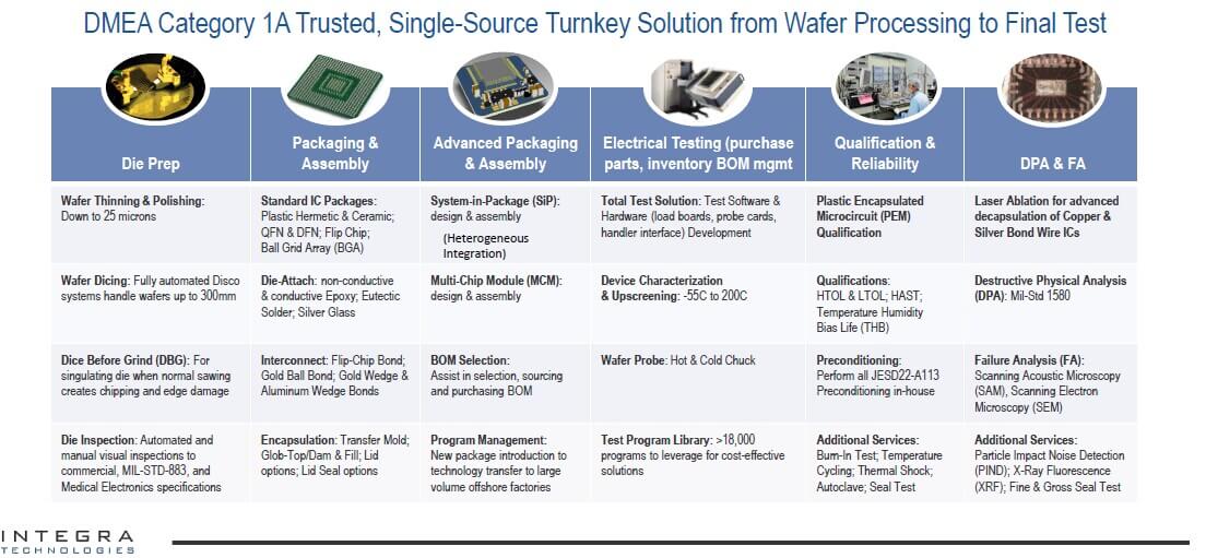
Matt Bergeron of Integra described the company as the largest US-owned and operated OSAT (Figure 1)
SkyWater
SkyWater’s Alan Huffman detailed the company’s plans to be the first US-based pure-play provider of silicon interposer, FOWLP and hybrid bonding heterogeneous integration and advanced packaging technologies. The company is ITAR-registered and capable of supporting secure applications with trusted accreditation in process.
As IFTLE has noted in the past through an IBAS program, they are completing a four-phase approach for scaling up the IMEC silicon interposer process at the BRIDG facility in Florida (Figure 3).
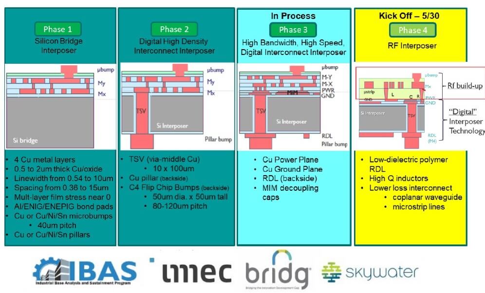
SkyWater licensed Deca’s M-Series process in Oct 2021 and Adeia’s hybrid bonding technologies (the original Ziptronix HB technology) in May 2022. (Figure 3 shows that Phase 1 was completed in 2022 and Phase 2 is nearing completion. A separate functional demonstrator program is also nearing fab completion. Phase 3 is in progress, and Phase 4 will focus on extending the initial process to include more routing layers and an RF version.

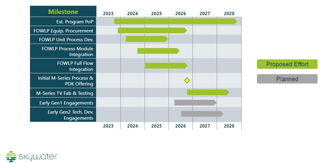
All FOWLP processes will be supported within Skywater FL. (i.e.: no outsourcing). The facility is being scaled for 1350 wafers/month. The FOWLP implementation roadmap is shown in Figure 4:
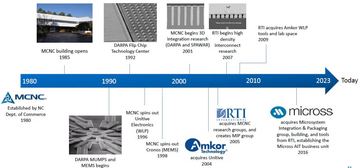
Micross
John Lannon gave an introduction to the Micross AIT (Adv Interconnect Tech) division. Its corporate evolution is shown in Figure 5.
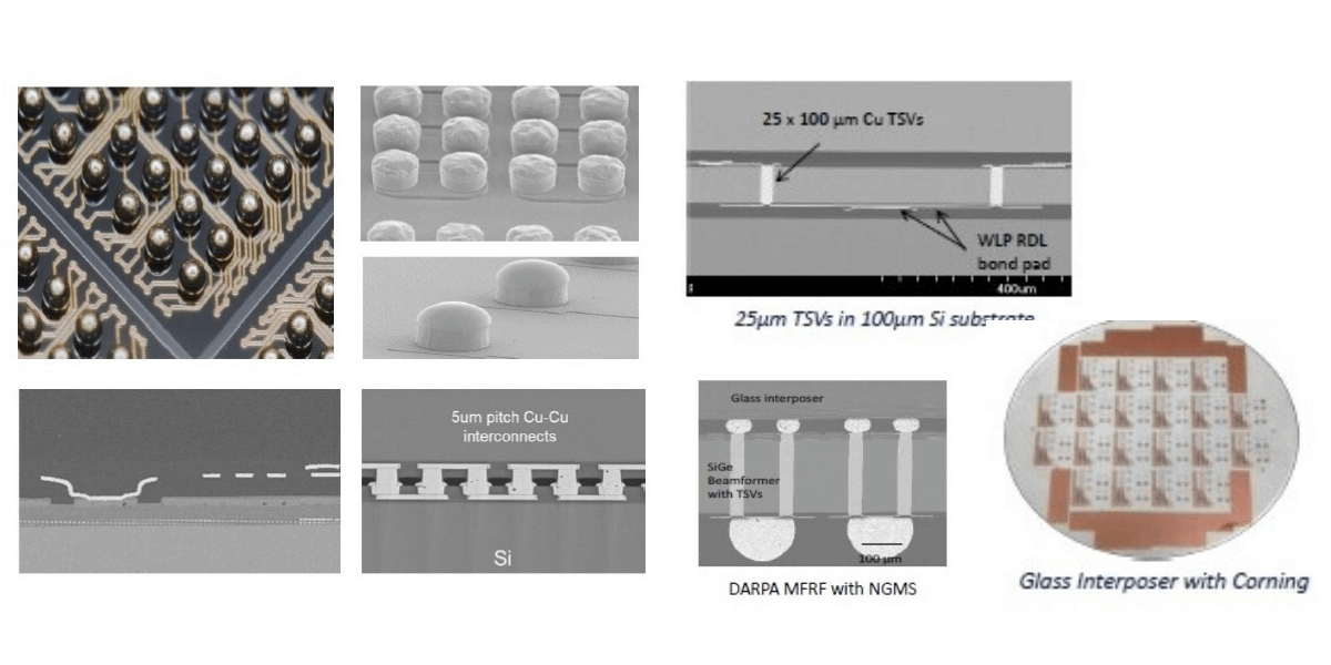
Some of the company’s current capabilities include:
- Wafer bumping
- Cu pillar
- Microbumping at sub 20µm pitch
- 5D Interposers using both Si and glass routing substrate
- 3D integration for via-last and via middle wafer finishing.
NHanced Semiconductor
 Bob Patti of NHanced Semiconductor detailed the company’s current hybrid bonding capabilities and plans for the expansion of its current North Carolina facility. The 25000 sq. ft. R&D fab features 7000 sq. feet of class 100 cleanroom space and focuses on what Patti calls “High Touch Manufacturing”, focused on process development and prototyping, including 2.5D and 3D manufacturing and the use of exotic materials. (Figure 7).
The facility supports 100, 150, and 200mm wafer processes including photolithography, etch, metallization, dielectrics, bonding, wafer thinning, CMP, as well as wafer-to-wafer and die-to-wafer bonding. The facility is also ITAR registered and ISO 9001-2015 certified.
The post’s feature photo shows the ribbon cutting at Nhanced Semiconductor’s Westgate IN facility (now under construction) is expected to be able to produce 50,000 wafer starts/month capacity (50X the current NC facility).
For all the latest in Advanced Packaging stay linked to IFTLE……………………………………

