
CHIPS Act Innovation Hubs
SEMI has published an interesting article where they predict 10 likely locations for CHIPS Act Innovation Hubs.
Aside from the CHIPS Acts $52B in subsidies for American chipmakers and 25% tax credits for capital expenditures, the Department of Commerce is also allocating $10B (over five years) for “20 geographically distributed regional technology and innovation hubs.” The location of these hubs is as yet unknown, but it is reported that at least three will be based in each of the six regions shown in the map in Figure 1.

I will let you read the article and determine for yourself whether these 10 make sense to you, but for the record, the authors are predicting the Phoenix area, Silicon Valley, Idaho (Boise area), Indiana (near Bloomington), Minnesota (near Skywater), NY (near GF), Ohio (near Intel), Oregon (near Intel), Austin TX and Virginia. Not really going out on a limb…are they?
Silicon Interposer Tech Development by SkyWater/BRIDG under DoD Funded IBAS Program
The Skywater/Bridge partnership has announced the completion of phase one of its DOD-funded Industrial Base Analysis and Sustainment (IBAS) technology development program.
Through its partnership with IMEC, SkyWater has developed a baseline fabrication flow for silicon interposers. The IBAS goal was/is to establish a comprehensive domestic silicon interposer manufacturing capability, supporting several advanced electronic systems. Phase one bridge interposer capability will also be used in subsequent phases of the silicon interposer development program, where through-silicon vias (TSV) and RF-enabling materials and devices will be incorporated. The technology will be available to both government and commercial customers.
Now, let’s continue our look at papers from the IMAPS International Symposium.
Samsung
I always try to look for a poster paper that shares some key information if you bother to spend the time to find it. From this conference, I selected the presentation “The Study of Highest Thickness Photo Resist for Cu Post of Fan-Out Wafer Level Packaging” by Samsung’s semiconductor development group.
The paper was focused on how Samsung developed a thick photoresist (>350um) but the interest to me was in their reasons for wanting it in the first place.
The limited thermal budget of mobile devices does not allow for the use of high-performance application processors (AP) at their full speed. Therefore, controlling the heat generation of the AP chip is becoming a key factor. Samsung feels it is necessary to increase the thickness of the AP dies without increasing the thickness of the AP package.
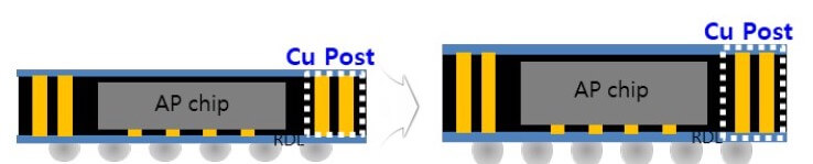
Due to the nature of the AP, DRAM (Memory) must be located as close as possible for high-capacity and high-speed operation, and to implement this, traditionally a package-on-package (PoP) structure is required. So, what is needed is to replace the PoP structure with a molded, thin RDL substrate with tall, Cu-post, through-package-vias (TPV) as interconnect. Such a package is shown in Figure 2, where the die thickness is over 200µm and the copper post > 300µm in the RDL-based fan-out package structure. The AP thermal resistance is thus reduced.
Siemens EDA
Bill Acito, of Siemens EDA (i.e. Mentor Graphics), shared with the audience his perspective on An Organic Package Designer’s Guide to Transitioning to FOWLP and 2.5D Design.
Where once there was a clear-cut delineation between the silicon die design and IC packaging design, we have now entered a design domain where silicon-based substrates, 2.5D, and 3D stacking technology are blurring the design domains between classic IC design and advanced packaging. Acito questions “Can the IC packaging design tools be used to design silicon substrates? Is silicon substrate design an IC design challenge or an IC packaging design challenge?”
Digital IC silicon layout tools tend to focus on a single die, and clearly, with the disaggregation of large SoCs and the advent of chiplet technology, systems with a large processor and multiple stacks of memory may not be a good match for a single-die-centric tool. A tool that can plan, manage, and analyze an entire system early in the design process is advantageous.
Packaging and PCB technology-based solutions focus on multi-component, system interconnects analysis and organization. PCB and packaging design technology take a system-level approach, optimized for multiple die, substrates, and discrete components.
Suppose the die components are not “off-the-shelf” and are in the process of being designed while the overall system is being designed. In that case, the system tool can leverage “co-design” between the die and the interposer or packaging domains to optimize chip I/O pad ring placement, substrate placement, and stacking organization to provide the shortest and best signal and power response as well as minimize the number of layers and the obstruction and congestions challenges when routing the design.
The ability to bring the system into a single planning tool can allow system-level SI/PI/thermal analysis and co-simulation across multiple fabrics and multiple layers accounting for the internal routing as well as the component interconnect.

Acito concludes that the IC packaging design tool set has matured to the point where it can address not only classic plastic, organic and ceramic packaging substrates but can also address silicon substrates driven by interposer and chiplet designs. In most cases, system and packaging teams do not have to abandon their existing toolset to support these designs. The packaging design tool set can offer additional capabilities concerning multi-component system design and component stacking better than an IC layout tool. Catch Bill’s podcast interview on the topic with Françoise here, beginning at 15:21.
Siliconware
SIliconware discusses the pros and cons of using high vs low-k dielectric constant (Dk) materials in antenna-in-package (AiP) structures.
The fifth generation of new radio (5G) technology is being actively researched where some frequency bands reach 28GHz (mmWave). When the frequency reaches a millimeter wave, the antenna can be designed into a package (AiP), since the antenna size becomes small enough due to the shorter wavelength, thus providing better integration into mobile devices.
Most designers understand that by using a substrate material with a higher Dk, the size of the microwave circuit can be miniaturized. The circuit size decreases as the Dk of the substrate material increases, allowing the millimeter-wave antennas to integrate into mobile devices more favorably. A typical structure is shown in Figure 3.
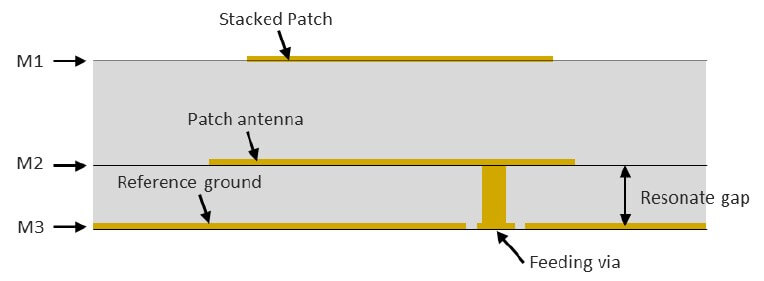
Siliconware workers designed and simulated a patch antenna with two materials of Dk – 3.4 and 6.3 at 28GHz in a 3-layer stack-up structure. Designing with 6.3 Dk results in a smaller (30%) width of the single antenna and a thinner (22% ) thickness of the resonator gap. In contrast, the peak gain is 15% higher with a low Dk of 3.4. The gain of the antenna array could be compensated by increasing the quantities of the antenna with higher material Dk in the same dimension. Thus, the design of the antenna with the proper selection of high Dk material can help to reduce the size of the antenna module and increase the radiation angle.
Henkel
Henkel detailed its studies on Silicone Migration Risks and Mitigation in Thermal Interface Materials, where they shared some interesting perspectives on issues that can occur with silicone-based materials.
Thermal interface materials (TIMs) usually comprise a compliant polymeric matrix with thermally conductive fillers. Silicone polymers are used for their thermal stability, relatively temperature-insensitive rheology, and mechanical properties. Polymeric TIM materials include (1) large, gelled clusters, (2) long and short polymer chains that are not chemically bound to the structure but entangled with it, and (3) volatilizable small molecules. The issues are with the latter, i.e. low molecular weight silicones that can volatilize and migrate through vapor phase migration and medium molecular weight silicones that can bleed out of the TIM through liquid phase migration. The rate of bleed depends on the temperature gradient. Once the material bleeds, the spreading is controlled by the surface tension of the bled material and its viscosity. Bled silicones with low surface tension and low viscosity can spread wide giving a perception of significant loss of material, even if the absolute amount is very small. While high volatility silicone low Mw components can be removed thermally, liquid migration is more complex both in terms of assessing risk but also qualifying a TIM, since this is application dependent.
Draper Labs
The Design of Wafer-level Solder Seals… was the topic under consideration by Draper Labs. Sealing large, heterogeneous assemblies at the wafer level presents a more challenging problem than sealing small individual sensors, primarily due to the wafer bow and irregularities in the seal surfaces.
While there are many types of wafer-level hermetic seals — such as gold-to-gold thermocompression bonding, gold-to-aluminum thermocompression bonding, glass-to-silicon anodic bonding, glass-to-ceramic using glass frit, and glass-to-glass using glass frit reflowed with a laser — the greatest number of wafer level hermetic seals have reportedly been made using various solder alloys. The reason for the preference of solder reflow sealing over the other techniques is that it has fewer process constraints. Thermocompression bonding requires the seal surfaces to be very smooth and flat. Glass frit seals require high-temperature oven reflow or laser transparent materials. Anodic bonds can only be made between silicon and cation-containing glasses and subject the parts to strong electric fields.
An often-touted advantage of solder bonding over other sealing techniques is that solder can bridge gaps between seal surfaces and accommodate non-planarity caused by wafer bow or conductor traces located beneath the seals.
Draper uses analytical and numerical calculations to investigate the interplay between seal width, height and shape of the seal gap, and solder volume associated with seal ring solder bonding.
For all the latest on Advanced Packaging stay linked to IFTLE…………………..


