


In its fourth edition and with a new name, the European 3D Summit (formerly the European 3D TSV Summit) reflected the shift from R&D to the real business of 3D integration and advanced packaging, and highlighted the significant growth this market space has undergone in the past year. It has also taken a new perspective, as we no longer view fan-out wafer level packaging (FOLWP) and 3D through silicon via (3DTSV) stacks as competitive technologies, and therefore adversaries; but as two classes of solutions that provide options to serve varied performance requirements at the lowest possible cost. Ultimately, his year’s event was all about the advanced packaging sector, in all its dimensions, as finally being acknowledged for the value it brings to the table. (Even Intel is acknowledging that multi-chip packaging is necessary to reach really high speed I/Os – as they announced at ISS that they will be starting to implement 2.5D and 3D packaging into processors this year).
In the early days of the march to 3D integration, this conference was more academic. Now, it has evolved into a business-focused conference as processes matured and are being integrated into products. Whereas we got used to seeing technology updates from a similar group of presenters and/or companies, this year there were only a few repeat presenters, and many new product-focused presentations on 3D integration for high performance computing products, imaging products, wearables, medical, MEMS integration, and more.
In addition to the market updates, which I will cover in more detail in a subsequent post, there was lots of discussion about 3D system-level integration, what’s driving it, and how it implements the whole spectrum of interconnect technologies including wire bond, flip chip, redistribution layers (RDL) and TSVs. Additionally, there were more references than ever before about advanced hybrid bonding, including Ziptronix’ DBI and DBI-like approaches being implemented into BSI 3D stacking, in addition to wafer-to-wafer and die-to-wafer bonding.
What wasn’t discussed at this conference was as notable as what was discussed.
Glass interposers, which in the past had merited its own session, came up only in passing, such as in the X-Fab presentation, because the company offers through glass vias (TGV); and briefly as part of the Yole Dévéloppement market update. Monolithic 3D IC, which has been a fairly hot topic for the past year or so since Leti introduced CoolCube, didn’t make an appearance at all. There was no discussion of test, or thermal management issues, nor solutions for either. This could be because as productization takes place, these issues have been solved by manufactures and have become a non-issue. Or there was nothing new to report. (Or maybe such topics just didn’t really fit into this year’s agenda, with so much other cool stuff to talk about.) And there were only two presentations devoted to design topics: Fraunhofer’s Andy Heinig stressed the need for assembly design kits (ADKs) that serve the same purpose for assembly as process design kits (PDKs) do for chip manufacturing; and Mentor Graphics’ demonstrated its experience in the chip/package/board co-design space aimed at satisfying that need.
We did revisit an old favorite with a new twist: temporary bond/debond. 3M presented new adhesives and processes they’ve been working on with SUSS MicroTec. Nanium and Amkor each talked talked about temporary bond/debond for FOWLP debond for thin wafer handling for FOWLP PoP configurations. Nanium is trading in its metal carrier for proprietary ceramic carriers for WLPoP, noted Steffen Kröhnert. This is because both glass and Si carriers don’t hold up to the debond process step due to the different properties of a reconstituted wafer. Conversely, David Hiner explained that as Amkor uses a chips-last vs. chips-first approach, the RDL is built right on the carrier, and the mold compound doesn’t come into play as part of the temporary bond/debond step.
Anne-Marie Dutron, general director of SEMI Grenoble and organizer of the event, said that expanding the focus resulted in more attendees, as well as from different sectors of the market. I weighed in with some of the attendees to get some additional feedback on the event and gain some insight from their perspective.

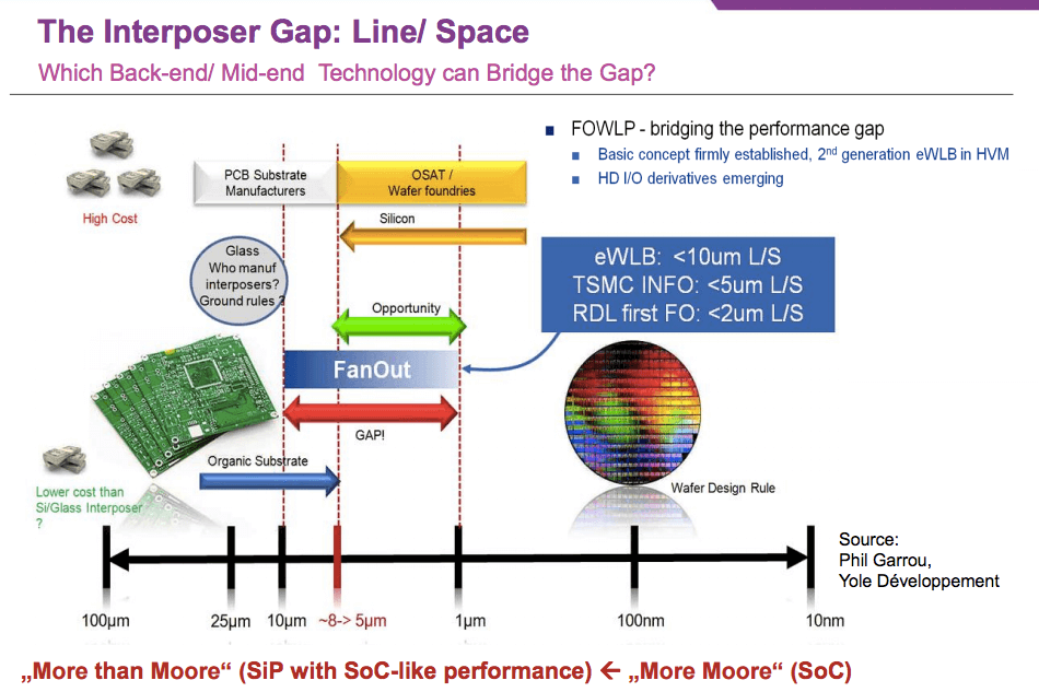
Even with the varied topics, Thomas Fries, FRT, commented that there was some redundancy throughout the presentations – for example with the multiple use of Phil Garrou’s now famous “mind the gap” slide (Figure 1). However, Fries noted that this wasn’t necessarily a bad thing; it’s an indication that we are approaching the mainstream with technology. Rather than technically detailed, there was more of a “mine is better than theirs” approach, as manufacturers vie for customer business. “It shows we are approaching some kind standardization in the industy,” he noted. “As a supplier of metrology solutions, this makes my life much easier.”
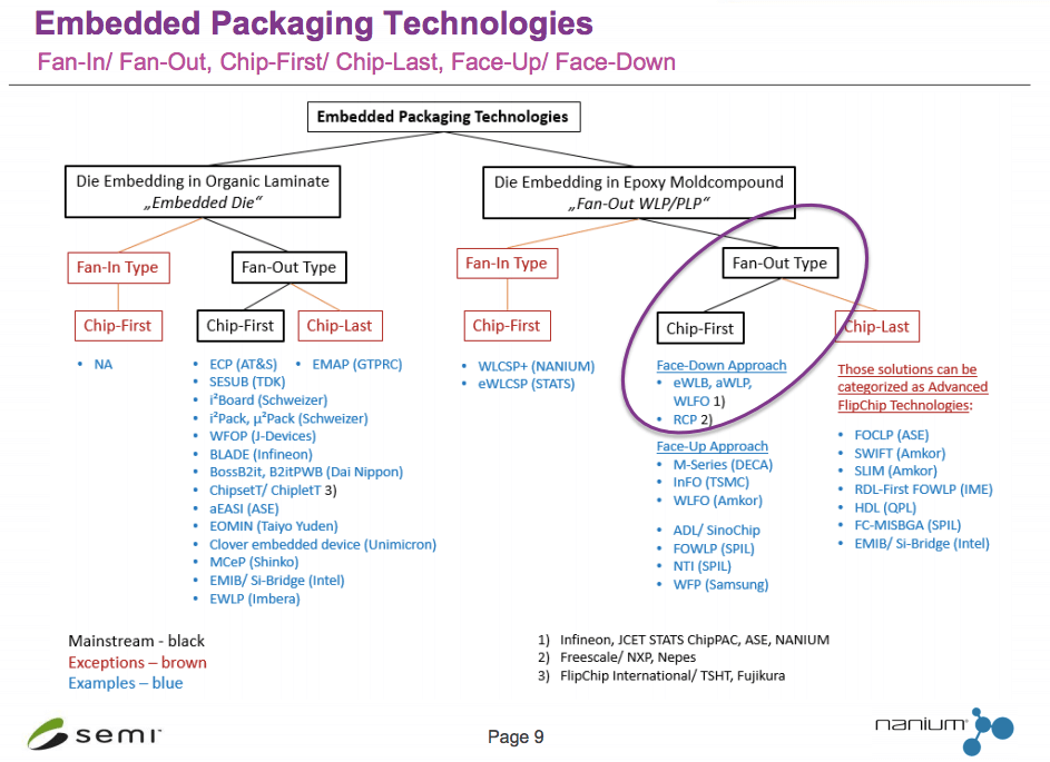
Tim Anderson, Fogale Nanotech, was a newcomer to the event, and offered some observations from that perspective. He said the presentation material was great, and overall appropriate to the topics. On the whole, as a veteran of front-end processes, he finds the whole packaging area very confusing. The terminology doesn’t truly fit what it is. The conference helped him to clarify and unscramble the scrabble board that falls under embedded packaging technologeis – with different companies changing up the terms to reflect different approaches, for example we have eWLB, WL-FO, SWIFT, SLIM, InFo, RCP, Chips-First, and SLIT, all variants of conventional and high density FOWLP (Figure 2).
For Ehrenfried Zschech, Fraunhofer IKTS, the main takeaway from the presentations of this year’s conference is that the increasing variety of 3D solutions, and therefore simultaneously the number of materials integrated in 3D stacks brings new challenges to reliability and requires study, particularly of thermal stress-induced effects.
Not long after I decided to focus on 3D packaging and start 3D InCites, it occurred to me that at some point, the third dimension would be a given in developing next-generation advanced packaging technologies. Because whether or not TSVs are involved, the third dimension certainly would be. This year’s European 3D Summit, from the name change to the content presented, was an indication to me that we are practically there. ~ FvT


