
Latest Posts
IFTLE 617: SK Hynix considers 2.5D packaging business with Amkor
Will TSMC, SK Hynix, and Amkor be an Onshore Source for Nvidia? SK Hynix learned to package its own stacked...
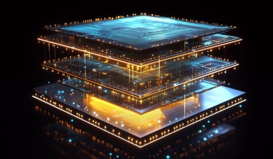
3D ICs Eliminate the Memory Wall
The adoption of 3D ICs allowed the elimination of the “Memory Wall” using a new memory architecture and through silicon...
Samsung’s 8GB HBM2 Becomes a Standard for Innovative Graphic Cards
In the AMD-NVIDIA battle, System Plus Consulting’s experts continue to pursue innovation and monitor progress. At the beginning of the...
Start Your 2.5D HBM Design Today
High-bandwidth memory (HBM) is a JEDEC-defined standard, dynamic random access memory (DRAM) technology that uses through-silicon vias (TSVs) to interconnect...
HBM Supply Chain Seminar Highlights System-level Advantages
The Computer History Museum in Mountain View is a very impressive place to show you the enormous progress ICs and...
The HBM Supply Chain is Open for Business!
Last June, AMD made 3D integration history with its introduction of the Fiji gaming processor unit (GPU), which for the... With 3D Memory Cubes You Can Finally Break Down the Dreaded Memory Wall
In July and August schools are closed and many people like to take vacation. Typically nothing major happens during these...
At AMD, Die Stacking Hits the Big Time
It’s official. Die stacking and interposer integration have been implemented in a high volume consumer application. AMD officially launched the...
IEDM 2014 3D Short Course Highlights 3D Memory Cubes for SYSTEM design
Years ago, when I gave my first 3D technology presentations, I noticed very different reactions from my diverse audience: The...

Highlights from HotChips 2014: 21 HBM Design-ins Ongoing!
Last week, HotChips 2014 (aka HC26) was held at the Flint Center within the De Anza College in Cupertino, California. As in...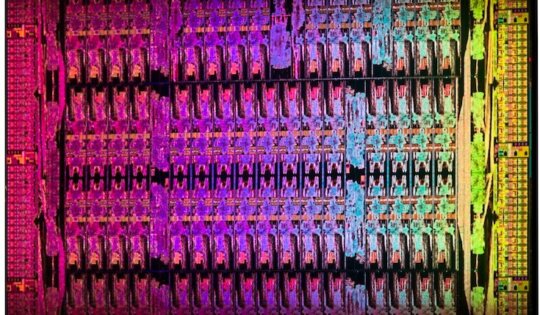
Intel’s Next-Gen Xeon Phi processor to have Micron 3D Memory Inside
Somehow in all my preparations for the 2014 3D InCites Awards and planning the schedule for SEMICON West this week,...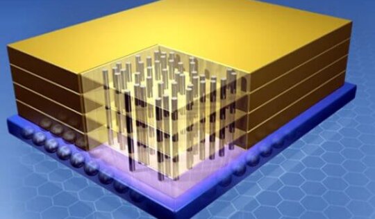
3D IC Adoption: What’s it going to Take?
If, as we heard at last week’s 3D IC Forum at SEMICON Singapore, that technology challenges and cost are no...
3D ASIP 2013: Coming Down The Home Stretch to 3D IC Commercialization
For years, we’ve been talking about the performance and power benefits of 2.5D and 3D ICs. We’ve also been talking...
IMAPS International 2013 3D Technology Highlights
Approximately 880 people registered for IMAPS International 2013, and yes the fiasco in Washington even affected IMAPS – there were...
The Many Flavors of 3D DRAM
Micron’s recent announcement that they will be shipping samples of the Hybrid Memory Cube (HMC) and ramping to production in...