

High-bandwidth memory (HBM) is a JEDEC-defined standard, dynamic random access memory (DRAM) technology that uses through-silicon vias (TSVs) to interconnect stacked DRAM die. In its first implementation, it is being integrated with a system-on-chip (SoC) logic die using 2.5D silicon interposer technology. In June 2015, AMD introduced its Fiji processor, the first HBM 2.5D design, which comprises a graphics processor unit (GPU) connected with four HBM stacks using a silicon-based interconnect.
The Fiji processor is powering AMD’s latest generation of Radeon Fury graphics cards for high-performance gaming. This event was the turning point for HBM, opening the floodgates for system integrators to adopt HBM as a memory solution for high-bandwidth, low-power products. In addition to graphics, HBM is being used in high-performance computing (HPC), data center and networking applications.
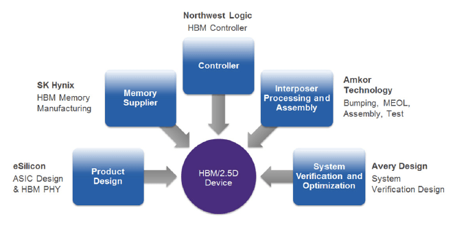
SK hynix Inc., Amkor Technology, Inc., eSilicon Corporation, Northwest Logic and Avery Design Systems have joined forces to offer a complete HBM supply chain solution that is delivering and supporting customer 2.5D HBM designs now. In this open supply chain collaboration,SK hynix provides the HBM stack. eSilicon is the application-specific integrated circuit (ASIC) vendor for the SoC, providing the HBM physical interfaces (PHYs) and associated services, and is also the overall HBM module integrator. Northwest Logic provides the HBM controller intellectual property (IP) for the SoC. Avery Design Systems provides the HBM verification IP. Amkor integrates the SoC, HBM stack and interposer into a 2.5D assembly, and tests, packages and ships it to the customer (Figure 1).
The five companies recently sponsored a seminar to promote their efforts and explain how this supply chain works. Attendee feedback was very positive and included the following comments:
- Bringing key players for interposer-based designs into one room was strategic and helpful.
It was very informative. I had a lot of questions answered
It was a good assembly of design and manufacturing elements.
I learned a lot that I didn’t know.

It’s good to hear that TSVs are ready for HBM.

This white paper explains HBM’s value proposition, and how these five companies make it easy for system and integrated circuit (IC) designers to access the many benefits this technology offers. Download the white paper here. You can also view the webinar here.
Authors
Kevin Tran, SK hynix Inc; Paul Silvestri, Amkor Technology, Inc.; Bill Isaacson, eSilicon Corporation; Brian Daellenbach, Northwest Logic; Chris Browy, Avery Design Systems.


Had attended that joint Webinar on 2.5 d back on Mar 29. Basic questions that were not addressed then were the gross metrics to evaluate the gain vs pain for going from baseline technologies ( packages on PCBs ) to HBM on 2.5 d interposer based designs. The metrics would be improvement in performance ( e,g. bandwidth, processor GFlops, sp. power for data transfer ) vs. additional cost. Those questions are not answered in the White Paper either.
P.S. : in that White Paper the AMD Radeon Fury Graphics module ( first commercial user of HBM on 2.5d ) is referred to as having given the green light to 2.5d, but neither the performance improvement nor costs are discussed.
Hello Dr. Gupta,
Below is an analysis done by Bill Isaacson, the eSilicon person who participated in the webinar. I think this will provide some good perspective.
Best regards,
Mike
• The correct comparison of HBM2 vs DDR4 is not $/bit, but rather $/bandwidth. The reasons:
• It is not practical to implement the equivalent bandwidth of HBM2 using DDR4. Assuming 16b DDR4 memories at 3.2Gbps/IO, you need 40 discrete DDR4 memories to have the equivalent bandwidth of 1 HBM memory. Assuming an average ddr4 interface is composed of 65 signals (ignoring power and ground), we would need 2560 package balls dedicated to the interface. This does not fit into today’s package technology. Additionally, you can put up to 4 HBM2 stacks in a package, providing even more bandwidth to the ASIC!
• Ignoring the previous point, let’s assume for a second DDR4 is feasible. The correct comparison is:
• DDR4
o 40 DDR4 memories
o Board space, assembly cost for these memories
o Multi layer board required to route to these memories (typically > 20 layers)
o On the asic, Silicon space for the DDR interface (>200 sqmm) —> this is PHY area only and doesn’t include the controller area.
o DDR4 interface power is in the 1 watt range per PHY, x 40 PHY = approximately 40W per ASIC.
• HBM
o 1 HBM2 memory
o No additional board space for the hbm2 memory, it’s embedded in the package.
o No additional board layers to escape route the memory
o On the asic, Silicon space for the HBM2 interface (~12 sqmm) —> this is PHY area only and doesn’t include the controller area.
o Additional cost of the interposer required to route between ASIC and HBM2.
o HBM2 interface power is in the 2 watt range per PHY = approximately 2 W per ASIC.
In this comparison, HBM2 is the clear winner, it’s not even close. HBM2 wins for performance (bandwidth), power, and cost when the design requires that bandwidth.