
If, as we heard at last week’s 3D IC Forum at SEMICON Singapore, that technology challenges and cost are no longer keeping 3D ICs from volume manufacturing, and indeed the key players are ready to go, then what’s it going to take to get this 3D IC adoption party started? It’s clearly becoming a matter of convincing SoC designers and system-level designers that 3D ICs offer cost benefits over 2D SoC, and power and performance benefits over traditional advanced packaging approaches.
According to Ramakanth Alapati, director of package architecture and customer technology group, GLOBALFOUNDRIES, there’s a cost penalty for modeling work, design methodologies aren’t there yet, and the design flow is in its preliminary stages. He says fabless companies like Qualcomm and Broadcom have solutions that work for them, and will continue to work for 2-3 years. “The drive isn’t there yet. It will come depending on how 14nm ramps,” he explained.“”If yield ramp is slow, that will drive the need for smaller partitioned die. Until there’s a need, it’s very hard for designers to intercept for split die designs.” He added that the drive will come from the “system guy” who wants to do something different in the market. The end customer (OEM) is looking at the overall performance cost. Getting the system cost savings message out to the OEMs and IDMs is tantamount to adoption.
As and integrated device manufacturer (IDM), IBM is one company that understands the system-level performance advantages of 3D ICs. Subramanian (Subu) Iyer, IBM Fellow, has been preaching the benefits of what he dubs “orthogonal scaling” for several years. In his early talks on orthogonal scaling, Iyer focused on 3D ICs as a scaling solution when we’ve reached the limits of CMOS scaling. His main message in his talk at the 3D IC forum was this: when you can’t scale the chip any more, you should start scaling the package and the board.
Iyer explained how today’s computer systems rely on memory locality. If a processor is working on certain data or instructions during one cycle, In the next cycle, all instructions and data reside where the previous cycle needed them. This is managed by a cache algorithm on processor chips. “70% of processor chips are caches, putting high density on chip memories at a premium,” he said. However, the world is changing and the amount of data to be stored and managed is colossal. Iyer says as a result, the old compute-centric model is moving to a data-centric model in which storage-class memory is surrounded by CPUs.
Iyer explained that scaling is not going to happen using conventional methods. While Si has continued to scale, circuit boards have not. “If we could scale the board down, we could achieve a 500x improvement in latency for the system, which would have a profound impact on its performance,” he explained.
Why is the board so big? Look at the package, he suggested. Packages today inflate the size of the die to match board pitches, and connect the chips to the outside world through a progressive fan-out. He said while the package protects the chip mechanically and thermally fairly well, with low-k materials, there are chip/package interconnect (CPI) issues that can destroy the chip. At 22nm technology, the fan-out pitch is 90µm.
So why are we doing this? Because the package has not scaled. While the industry has managed to scale Si technology by a factor of 1000 since 1969, the package has scaled by a factor of 3. Why is that? Presumably because of package cost. But when you consider the exorbitant cost of scaling Si — $200M for one EUV tool, and 1100 EUV tools are needed to supply the world’s requirement of Si in the 10nm timeframe — package cost isn’t so high. “CapEx for an OSAT is $40M,” said Iyer. “That won’t even buy a set of masks for an EUV tool.”

Iyer says the game is changing dramatically. We have to change the package philosophy from a necessary commodity to something that adds tremendous value. We have to scale the package and the board, and 2.5D and 3D are factors that make this revolution possible.
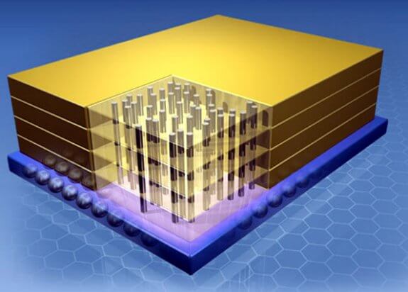
He pointed to the Hybrid Memory Cube (HMC) – for which IBM has provided the Logic and Micron, the memory stack – as an example of orthogonal scaling. The bottom chip of the HMC is a 32nm technology logic chip. All higher power logic functions, including I/Os are localized to the single logic chip on the bottom, for 1.28TB of performance. Ultimately, when compared to today’s technologies, he said the HMC:
- Has 85% less active signals compared to DD3
- Uses 90% less board space than DD4
- Consumes 72% less power than DDR4
Iyer noted that both HMC and JEDEC high bandwidth memory (HBM) will change the way we design memory into our systems. Both approaches may need new interposer/board solutions and allow for simpler chips. He also said that most of the processing for 3D ICs needs to be done in the fab because of fine features. “There’s a dramatic difference between the feature sizes of TSVs and feature sizes on a chip,” he noted. “Die stacking is the first step. But it’s not necessarily the best way to accomplish 3D. We have to go to wafer level stacking. With TSVs at the right pitch, we will be able to shrink the board.”
“I believe the productivity gains of package and board scaling we will get will be comparable to the gains we’ve had over the past couple years by scaling silicon,” concluded Iyer. So chip and system designers take note. It’s time to get on board. This is how we will build systems in the future! ~ F.v.T.


shifting goals
Not surprising what Subu from IBM had to say at the latest conference on 3d. IBM has always had a more mature & system level approach to cost, whereas chip makers have to focus on their one single chip or maybe a chipset, so the design & cost of systems using those chips may turn out to be sub-optimal. But its the total cost of a system ( chip, package, board, test, design, yield, software ) to deliver a target performance ( speed, power, size, reliability ) that matters. Perhaps at least the larger vendors of consumer systems today can afford to emulate ( and profit ) from IBMs systems approach to engineering hardware.
A case in point is battery power consumption & battery life of Smart Phones from two leading vendors. One gets away by putting in its Phones Batteries that have capacity ( mAh ) only about 60 % of the 2nd brand ! To access the Internet ( which requires all the graphics, digital and RF components to be fired up ) the first brand needs only 80 % of power compared to the 2nd one. This is possible only because the 1st brand does a better job of system optimization, starting with designing their own Application Processor.