
With two 3D focused keynotes and a 3D panel discussion, 3D Thursday was ripe for the tweeting. The sound bites were coming fast and furious from Subu Iyer, IBM Fellow, and Rao Tummala, director of Georgia Tech’s 3D Packaging Research Center. Additionally, the 3D Panel featuring both Iyer and Tummala, along with Jeff Brighton, Texas Instruments; Ron Huemoeller, Amkor; Nagesh Vodrahalli, Altera; Iyer; and moderated by John Lau, ITRI, provided some noteworthy take-aways.
Listening to Subu Iyer @IBM at #IMAPS. #3D and scaling go hand in hand.
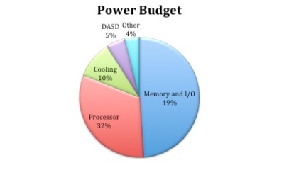
Anything you do with a scaled chip is going to be better with #3Di
IBM Fellow Subu Iyer was one of two keynoters on 3D Thursday at IMAPS 2012. He talked about Orthogonal Scaling, which includes embedded DRAM, on-chip power and delivery, and 3D Integration. In contrast to classical scaling, which focuses on reducing feature sizes, he explained that “an orthogonal feature is something you can add to existing technology with minimal or no effect to the existing structure.”
He identified power reduction as the most important improvement that can be addressed with orthogonal scaling. The total amount of power available (ie: out of the wall socket) for a system is constant. Communication between chips can take up to a third of a systems power (Figure 1). “Where does the power go? Mostly chips talking to other chips. Power used for cooling is a total waste,” said Iyer. “Semiconductor scaling does not address the power budget issue, but tighter inter-chip connections can!”
Iyer talked about a vision for 3D stacking and system on interposer technology. He said there’s a lot to be gained by Flash and DRAM memory in large quantities so the connections are made through short wires rather than expensive DDR protocols.
He also said you can get the same transistor count in 22nm technology using 3D stacking as 14nm. However, he cautions that 3D does not make the transistor smaller, faster and lower power. So that’s what makes it an orthogonal element. You still have to continue scaling.

Iyer didn’t leave out manufacturing hurdles. For example, where TSVs connect in the hierarchical wiring scheme is a key manufacturing issue. Putting small TSVs at lower levels is difficult because of the size mismatch between TSVs (huge!) and other features (really small). On the other hand, putting TSVs high in the stack blocks wiring. Ideally, he suggested putting them at the 10x level to get the best of both worlds. Another issue that will plague us, says Iyer, is wafer bow. Top and bottom die (or die and interposer) need to work in tandem to zero out effects at every stage in the assembly process, which will require a certain level of intimacy between the die supplier and the assembly house. In other words, secret sauces need to be revealed to make things work together seamlessly. He ticked off the usual laundry list of remaining challenges: grinding, temporary bond/debond, test, reworkability. Regardless, Iyer says he believes we can get there. “There are a lot of things happening in the world that makes me think we can actually do this,” he said. “It’s a cake walk compared to embedded DRAM.”
Georgia Tech’s Rao Tummala says the #iPhone is a packaging miracle, what’s inside is not due to system scaling. #IMAPs
Just think of what density improvements can be made to the #iPhone thru true system scaling! #gtechprc #IMAPS #3DInCites
We talk a lot about scaling at the die level and package level without giving much thought to what makes up the rest of a smart system. Tummala’s talk focused on the bigger picture. “Smart systems require a new paradigm.” He explained, “It requires scaling at the system level as opposed to simply the transistor level.” The current approach – for example, the manufacturing of the iPhone – leads to low functional density. Using the technologies emerging today, Tummala says we have the opportunity to bridge a system scaling gap of 106 and improve functional density. For example:
- Ultrathin glass interposers (<30µm) in roll-to-roll format
- The ability to make 1000 through glass vias (TGVs) in one shot
- Nanoscale interconnects
- 3D Silicon and glass integrated passive devices (3D IPDs) that have components on both sides.
- Thermal technologies are also turning to system scaling technologies with microfluidics, micro-channels, carbon nanotubes, and nano-TIMS.
- Nanoscale batteries are in development using thin-film technologies.
Tummala also suggested the package as the system. “If we can’t design and build an entire system on a large chip, why not on a small package?” he queried. But how to deal with engineering challenges and rework on these very thin copper-to-copper interconnects? “Think of everything like an IC.” We have to produce high-yield perfect manufacturing that is so small and cheap, that we don’t test it. If it doesn’t work, throw it away.
@TXInstruments Jeff Brighton, #3DIC fundamental decisions are behind us it’s a matter of taking good capability and making it great #IMAPS
And so opened the 3D Panel Discussion “Are Supply Chains Ready for 3D Integration Manufacturing?” This has been a recurrent panel theme over the past year. I’ve attended most of them, and what I’m discovering is that there are as many opinions about this as there are a variety of semiconductor packages. The main issues continure to be Who does what? Who owns the problems? How do we reduce cost?
Jeff Brighton, a self-described optimist, said, “we can seriously envision what 3D is going to be when it ramps to production.” Two years ago, there were still lots of decisions to be made. Now they’ve proven CMOS TSVs at 28nm can be done at high yield. Fab equipment is there. Metrology and inspection are no longer a problem. “All the fundamental decisions are behind us. It’s a matter of taking today’s good capability and making it great, No doubt in a couple of years, we’ll be ready to go!” (Gulp: a couple of YEARS?)
Nagesh Vodrahalli said he was a realist, and that Altera’s interest in 2.5D is for the functional integration it enables when you want to combine memories, third party and/or user-customizable ASICS, and optical interfaces. He’s of the mind that manufacturing issues are engineering challenges and not technology showstoppers. The bottom line is still cost. Vodrahalli says the solution needs to be at cost parity with today’s systems while providing higher functionality. “Collaboration in the supply chain is what will make this work.” He said. “It’s something that hasn’t been done in the past, but cost will come down if there’s collaboration across the supply chain.”
There was lots of discourse around how much of 3D is suited to the foundry and how much is a packaging service and who owns the liability. Iyer said that due to the level of cleanliness not generally found in a packaging facility, a significant investment by the OSATs will be required to accommodate it. Alternatively, it can all be done in the fab.
Then there’s the issue of memory. “No DRAM vendor will ever give out test vectors, and there will never be a 3rd party testing DRAM,” he said, adding that he doesn’t see the attitude changing quickly. With 2.5D, he said we can “muddle our way through,” but with 3D top and bottom die being more sophisticated, “IDMS will lead the way.”
Huemoeller said collaborative alliance is the key to enabling the 3D ecosystem. With regard to DRAM liability, he offered an OSAT perspective: “We don’t feel good about buying memory. The IDM or OEM ultimately owns the responsibility.” This aligns with Qualcomm’s vision of the PoP – like business model. Speaking for Altera, Vadrahalla said, “We do the design, we own the responsibility.” Brighton said the customer buys the memory. Iyer noted that in the IDM world, there’s no contention of ownership.
While Vadrahalla mentioned the need for cost parity, Tummala was much more direct. “I’ll say it one more time. 2.5D and 3D are too expensive. What can be done to lower the cost?”
Iyer noted that TSVs are a fab process, and add only 1-2% to wafer cost. The issue is with the backside processing. The foundry perspective is that they already do those things, it provides a reutilization of existing tools. Whereas the OSAT needs to invest in a new toolset. Brighton said it’s not that obvious, and that multiple OSATS are developing backside finish processes successfully. Vadrahalli suggested an alternative to lower the cost of 2.5D by third party providing the interposers. ‘There’s a great market for someone to step into and just produce interposers for anyone who needs them.” Brighton noted that at the end of the day, a customer will buy the lowest cost solution to the problem they are trying to solve.
Here’s what I think. While we continue to hash and rehash these issues and predict production dates for the benefit of conference attendees (and to give me and other journalists and bloggers something to write about) real work is already happening behind closed doors, and it will be the ones NOT talking about it that suddenly introduce a 3D product. ~ F.v.T.


