Years ago, when I gave my first 3D technology presentations, I noticed very different reactions from my diverse audience:
- The packaging engineers were in their element, engaged right away and asked detailed technical questions.
- The IC designers appeared quite worried about the strange — and for them, at that time — very different new challenges.
- The system designers followed very attentively every word I said and typically asked afterwards in disbelief: “Are you trying to tell us that this new technology will enable us to double system speed AND cut power dissipation by 50%???”
Let’s fast-forward about 5 years and quickly summarize what these three camps and I have learned in the meantime.
- The packaging experts’ initial reactions were spot on: YES, thermal challenges are the #1 technical problem for 3D-ICs and more manageable in interposer-based designs.
- Many IC designers already went through a steep learning curve to become familiar with the benefits and challenges of partitioning designs and packing multiple dice into a single package — mostly side-by-side on an interposer.
- The system designers now believe in this new technology, know that they can more than double their systems’ speeds AND cut power by more than half, therefor can’t wait to take advantage of the performance versus power ratios, bandwidth and latency gains, ease of heterogeneous integration, form-factor reductions and other benefits interposer designs and 3D ICs can offer.
And what did I learn? 3D technology is much more complicated than I expected and after 6 long years of development, only memory cubes are really ready for high volume production. A number of technical reasons, very complex business reasons and of course the worst recession in our lifetimes forced many of us to be cautious and advance slowly into the 3D-IC world – UNTIL NOW.
After this lengthy intro and a look back, let’s focus on the present and talk about what I learned about the promising future for 3D technology at IEDM 2014 3D Short Course.
This Short Course, titled “3D System Integration” exceeded by far my expectations and clearly confirmed my predictions that 3D memory cubes are destined to change the market dynamic for 3D technology. Here are a few highlights:
After a brief introduction by IMEC’s Eric Beyne, the organizer of this Short Course, Denis Dutoit, Research Engineer at CEA-Leti, gave a very good overview what 3D technology can offer system designers as well as what kind of applications are and will be the killer applications for 3D technology, especially 3D memory cubes.

The above slide (Figure 1) summarizes the key objectives a system designer will have to consider: Performance (versus power), form factor and (system) cost. While I expect that interposer designs will capture a much larger part of – especially heterogeneous – system designs then shown above, I really like how Denis highlights the key 3D components for system designers.
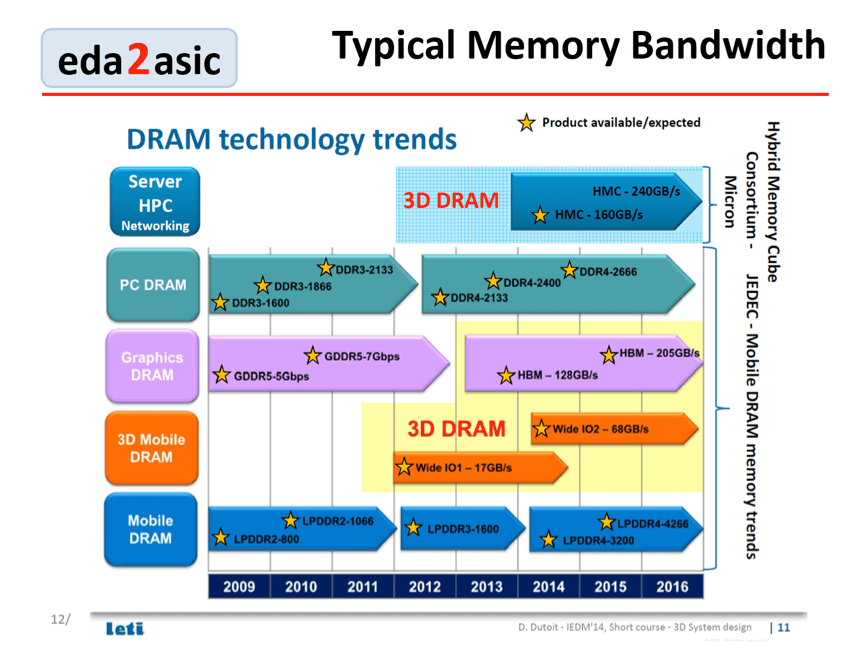
Another one of Denis’ slides caught my eye (Figure 2). In it, he summarizes the available/expected DRAM technologies. Using a slide from Nvidia, I showed in a previous blog that DDR4 and even GDDR5 can’t deliver the bandwidth needed for the next generation graphics solutions. High Bandwidth Memory (HBM), with its very wide data-bus (1000 lanes), comes to the rescue.
Likewise, high-performance computing needs larger and larger amounts of memory and more bandwidth than DDR technology can offer, and initial designs have demonstrated that the Hybrid Memory Cube (HMC) fits the bill very well.
In addition, the high-volume mobile applications need more bandwidth for streaming HD video. Wide I/O 2 is technically well suited for this market and potential uses, but needs to offer lower cost, before this concept can be deployed in volumes.

All three application areas will enjoy several times higher bandwidths and the significantly reduced power consumption that HMC, HBM and Wide I/O 2 offer, compared to the established DDR solutions.
Dutoit also presented a number of examples to show how the very wide busses 3D technology enables can benefit system architectures, talked about the 3D design solutions Cadence and Mentor offer, showed how Atrenta’s Pathfinding tool works, covered TSV modeling, Ansys’ power integrity tool, Docea’s power estimation capabilities, outlined the ongoing 3D test development programs, Si2’s data exchange and interoperability standards efforts and mentioned STMicroelectronics and several others as important 3D development partners for Leti.
Knowing Subramanien Iyer for many years, I was looking forward to his presentation. He is an IBM Fellow and Director of IBM’s System Scaling Technology. Subu also spoke from a system architect’s perspective about the capabilities of 3D technology. He demonstrated that 3D memory cubes can reduce system power by up to 75%, versus DIMM strips, and showed an excellent example how memory access time / latency can waste processor cycles and power (Figure 3) Iyer also explained how to partition and implement a system for maximizing the 3D benefits and allowed us a peek into IBM’s vast knowledge base in high-end computing and IBM’s experience with very large chips.
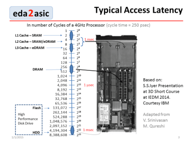
This slide visualizes how powerful CPUs on a server blade are sitting idle for thousands and even millions of clock cycles when they need to fetch instructions or data from different types of external memories. Packing CPUs and memory cubes very close together, e.g. on an interposer, can reduce these expensive “wait states” by several orders of magnitude AND reduce system power dissipation.
In addition to these two design-centric presentations, the Short Course also included 3D manufacturing focused presentations from IMEC’s Kristof Kroes, RPI’s James Jian-Qiang Lu and Kangwook Lee from Tohoku University. These experts demonstrated that the development of reliable and cost-effective manufacturing technologies is progressing well. The memory cubes mentioned above will give our industry plenty of manufacturing experience to continuously improve 3D design, as well as the manufacturing flows to enable the system designers to finally more than double performance AND to cut system power into less than half.
I have been riding the 3D Train for more than 6 years so far, and really enjoy working with so many very smart people riding with me into a new and very compelling semiconductor paradigm: Interposer-based and 3D-ICs.
HAPPY NEW YEAR! ~ Herb