
For years, we’ve been talking about the performance and power benefits of 2.5D and 3D ICs. We’ve also been talking about the remaining challenges, and have steadily ticked off the technology-related ones. The “elephant-in-the-room” has been, and continues to be cost. But based on the messages of some key industry players who presented at this year’ 3D Architecture’s for Semiconductor Integration and Packaging (3D ASIP 2013), it looks like while we continue to find ways to chip away at cost, we’re also beginning to accept the inevitable: yes, 3D ICs are going to cost more than wire bond and flip chip packages. But guess what? They just might be worth it.
In his opening keynote, Doug Yu, Sr. director of integrated interconnect and packaging, TSMC, noted that scaling system on a chip (SoC) is facing tremendous challenges, and its time for a paradigm shift to system scaling via system-in-package technologies. “We need to move to wafer level system integration (WLSI) to solve the problems of increasing transistor density,” he said. Yu pointed mainly to the market shift from PC to mobile products as the driving force. In the PC days, he said, we needed faster, faster, and faster devices and pursued Moore’s Law. For mobile, optimal system needs include not just speed, but cost, power and form factor requirements. “We need quick, simplified integration to catch the market,” he explained. “Innovation integration and leverage is what WLSI is all about.” All advanced packaging approaches, including 3D ICs, 2.5D interposer technologies like TSMC’s chip on wafer on substrate (CoWoS), and fan-out wafer level packaging (FOWLP), are needed and Yu believes this can be done with WLSI.
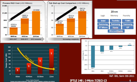
In his 3D IC status report, Phil Garrou shared some charts and graphs that demonstrated the economics of scaling to further nodes to explain why TSV is a cost saver over scaling to further nodes. It’s clear that due to disparate profit margins, TSVs are a more attractive option for the foundries than the OSATs. Until the cost of TSVs come down, the OSATS would rather reduce specifications and do with less performance at a lower price. What I find myself wondering is, will the OSATS ultimately lose out on this if they don’t add capacity to handle TSV assembly processes?
Doug Yu explained to me that while the cost of scaling is increasing as we move to the next node, we can’t disregard the lost real estate (and therefore added cost) due to keep-out-zones (KOZ) required when using TSVs. So while TSMC has invested heavily to offer advanced packaging process to its customers, it’s not abandoning further scaling altogether. Offering end-to-end services is part of the company’s strategy to provide customers will all the options available. This is also why TSMC has adopted an open innovation platform.
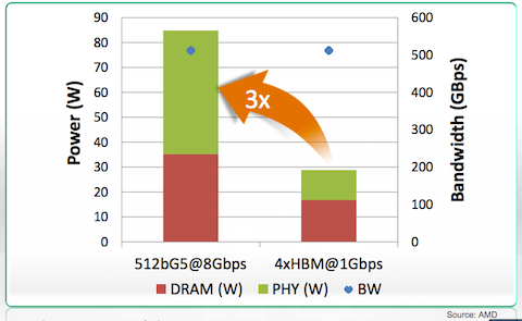
No presentation at 3D ASIP 2013 was more compelling or clearer on the reasons for shifting to 3D TSVs than Bryan Black’s, of AMD. Black said he’s been silent for 7 or 8 years about die stacking because “I didn’t want to say anything until I had something exciting to talk about.” That time is now, and he revealed that AMD has been working on high bandwidth memory (HBM) DRAM with Hynix, and that the first generation of HBM is sampling. “Hynix is aggressively ready to go into production with these things, and AMD is there to support them,” he announced.
Black prefaced his announcement with the statement, “Nobody will do it (TSVs) until they absolutely have to, or until it will pull them into a market segment they can’t get into any other way. The ‘absolutely have to’ is here. And AMD is going to do something soon.” He said HBM DRAM will bring TSVs into mainstream computing, and ultimately into the compute component of the phone, which up until now has seen TSVs only in image sensor and MEMS devices.

“The coolness of this, is that it completely changes how we use devices,” noted Black. “When we don’t have a new form factor for a while, things get boring and the industry stagnates.”
Black said that while cost is the primary motivation for integration, Si integration is running out of gas. All similar technology components have been integrated. “We can’t integrate disparate technologies such as DRAM, MEMS, True IVR, storage and optics into an SoC,” he said. “Moore’s Law will continue, but there are long-term cost challenges that will slow the adoption of the next process node.” Every time we drop a node, mask count climbs; defect density increases and yields drop. To avoid the high curve, companies will figure out how to stay in older process nodes longer, but still have to add value. “All TSV does is put disparate die closer together and makes them look like they’re on the same die.”
And while TSVs are admittedly expensive, its not going to be expensive for long, says Black. “There’s nothing special about the technology. It’s just scary. Once we get over the scary, there will be a drop in pricing. Then when volumes go up, there will be another drop in pricing as companies dedicate lines. In 3-4 years, it’s going to be cheap,” predicts Black.
Other presentations of note at this year’s 3DASIP: Jan Vardaman’s 3D readiness report card, updates on interposers, and a number of approaches for cost reduction on TSVs. So look forward to more coverage of 3D ASIP 2013 over the next few days. It looks like exciting times are still ahead for 3D integration. ~ F.v.T.


