

The 3D Architectures for Semiconductor Integration and Packaging (3D ASIP) conference is one of the biggest (if not THE biggest) event focused exclusively on the 3D IC family of technologies. The December 2016 event was held even closer to San Francisco airport than in previous years. From the lobby of the SFO Marriott Hotel, we could see planes taking off and landing. Every smooth touch-down and elegant take-off confirmed how advanced airliners serve today’s travel needs.
Yes, it took about 100 years to progress from the Wright brothers’ first flight to today’s state of the art. Likewise, the automotive industry also took ~100 years to advance from Ford’s Model-T to today’s luxury sedans and SUVs.
How did Boeing, Airbus, GM, Ford and many other system manufacturers reach today’s state of the art? They realized that the integrated device maker (IDM) model’s limitations hamper both technical progress and profitability. They formed partnerships and structured supply chains to focus development expertise and leverage economies of scale.
The semiconductor industry came to the same conclusion in the 1980s and has had to make many changes in the last 30+ years to disintegrate most big IDMs into fabless IC vendors, foundries, and assembly houses as well as EDA vendors and soft/hard IP suppliers. They also had to define new business models as well as sign-off criteria between these companies.
I had opportunities to contribute to process design kit (PDK) developments, TSMC’s design reference flows, and the roll-out of several ARM IP cores. I saw first-hand how these three offerings enabled IC designers to quickly simulate their ideas and present them to management for project approval, design, and release to manufacturing.
At 3D ASIP 2016 I really enjoyed hearing about the impressive progress assembly houses, equipment vendors, and material suppliers have made. In addition, I was really surprised by how widely wafer stacking is used in image sensor manufacturing for a broad range of digital cameras.
However, I was expecting to see more IC and system vendors – the actual 3D-IC customers – at the conference. Also, I missed the enthusiastic discussions between suppliers and customers common in the GSA’s 3D Working Group meetings I organized from early 2008 until the end of 2011.
Please, don’t misunderstand, 3D ASIP 2016 was a well-organized and very informative conference, in a convenient location, with excellent speakers outlining their capabilities and investments to cost-reduce their products. I counted 37 manufacturing and product centric presentations and, including my own, three design-centric messages. This ratio indicates that the bridge comprising EDA design flows, assembly design kits (ADKs), and die-level IP between the many experienced 2.5/3D-IC manufacturers and potential customers is still very narrow.
Based on my experience with rolling out FPGAs, bipolar and CMOS gate arrays, cell-based ICs, and SOI technology, I am convinced that we need to complement the large investments already made in 2.5/3D IC manufacturing and wafer-level packaging with much smaller amounts of money allocated to the development of ADKs, reference design flows and die-level IP building blocks. Only then will we enable a broad range of customers to start many more 2.5/3D/WLP designs, secure returns on the large investments already made, and quickly recapture the relatively small investments still to be made.
Enough said about my objective to bridge the gap between EDA and manufacturing ASICs and other ICs. Let me highlight now some of the many excellent presentations.
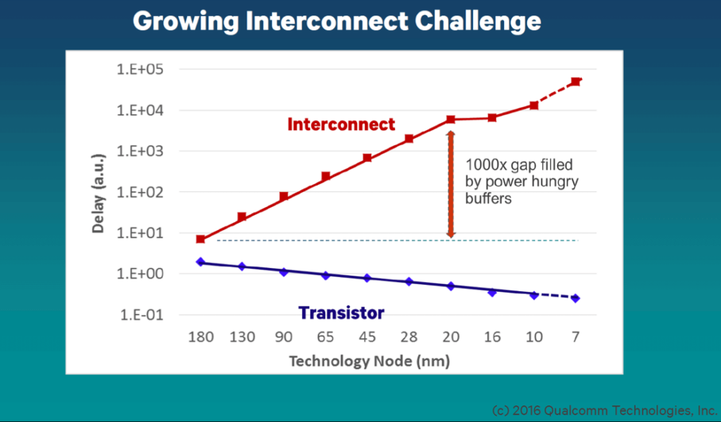
A very prominent IC vendor, Qualcomm, was represented by Yang Du from their research department. He conveyed why our two-dimensional SoCs will not be able to meet future performance and power requirements. Du also stated that – from his perspective – sequential 3D processing (also called monolithic, like 3D NANDs and Leti’s CoolCubes are using) and direct bonding (like DBI, Invensas offers) are the most important technologies for the success of 3D ICs.
Leti’s Pascal Vivet, chair of the design session, gave me the opportunity to be his first speaker.
I, of course, tried to convey my concerns outlined earlier in this blog and explicitly asked the many manufacturing experts in the audience to work closer with the EDA vendors (represented by Mentor’s Juan Rey, Cadence’s Brandon Wang and half of myself – my other half is solidly in the manufacturing camp!). I encouraged both sides to work together on ADKs and design flows because I have seen how these two capabilities contributed to making TSMC’s wafer fabs successful.
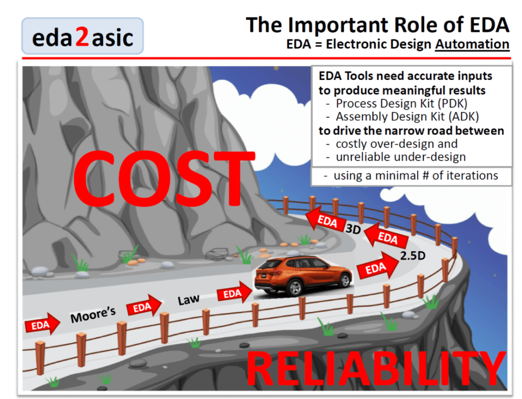
By presenting Figure 2, I re-emphasized that IC and system designers need EDA tools, and accurate inputs from manufacturing, to walk the fine line between costly over-design and unreliable under-design, earn project approval and funding, then get their designs to manufacturing on schedule.
Juan Ray focused his 3D ASIP presentation on how Mentor Graphics addresses general 2.5/3D design challenges, like chip and package co-design. He suggested expanding the current PDKs with package and assembly information to meet the die-package co-design requirements. Ray also talked about parasitic extraction and verification with “Calibre 3D”, outlined “Sahara’s” thermal analysis capabilities, how to analyze stress effects with “Glacier” and how Mentor and Leti are working together to address EM challenges in TSVs, RDLs, and wafer-to-wafer bonding.
Denis Dutoit described Leti’s vision for how system designers can use “chiplets” (die-level IP building blocks, also called “dielets”) to quickly assemble complex subsystems on active or passive interposers. To demonstrate how powerful this concept is, Dutoit described their design steps for a 3DNoC. He also showed some of Leti’s contributions to the European ExaNoDe (Exascale Processor & Memory Node Design) and talked about the power of photonic interconnects as well as Leti’s work on multi-die IC design flows with EDA partners.
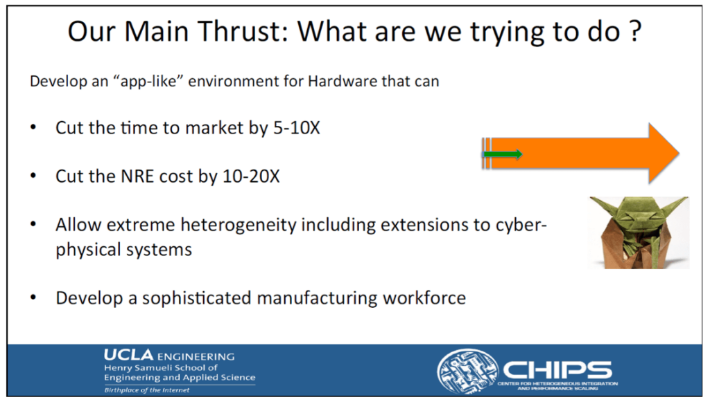
Prof. Subramanian Iyer outlined his work at UCLA’s “CHIPS” (Center for Heterogeneous Integration and Performance Scaling). “Dielets”, manufactured in the technically most suitable and lowest cost process technology when combined on an interposer, minimize form factor, interconnect delays and power. Based on his many years of experience at IBM managing ultra-complex high-performance chip designs, Iyer shared his vision how die-level integration of heterogeneous functions will impact electronic system design in future. The key objectives of the CHIPS program are outlined in Figure 3.
Among the many other great presentations, the very visionary message from ASE’s Bill Chen really impressed me. His Keynote was about the new Heterogeneous Integration Roadmap (HIR). After many years of contributing to the now discontinued International Technology Roadmap for Semiconductors (ITRS), Chen reasoned how the increasing risks and cost of continued shrinking and the growing market demand for integration of heterogeneous functions, suggested replacing the ITRS efforts with the newly formed HIR team.

Also, the presentations of John Hunt and Rich Rice showed that ASE is fully prepared to offer customers advanced packaging technologies to add value and differentiation to their ICs and (sub)systems.
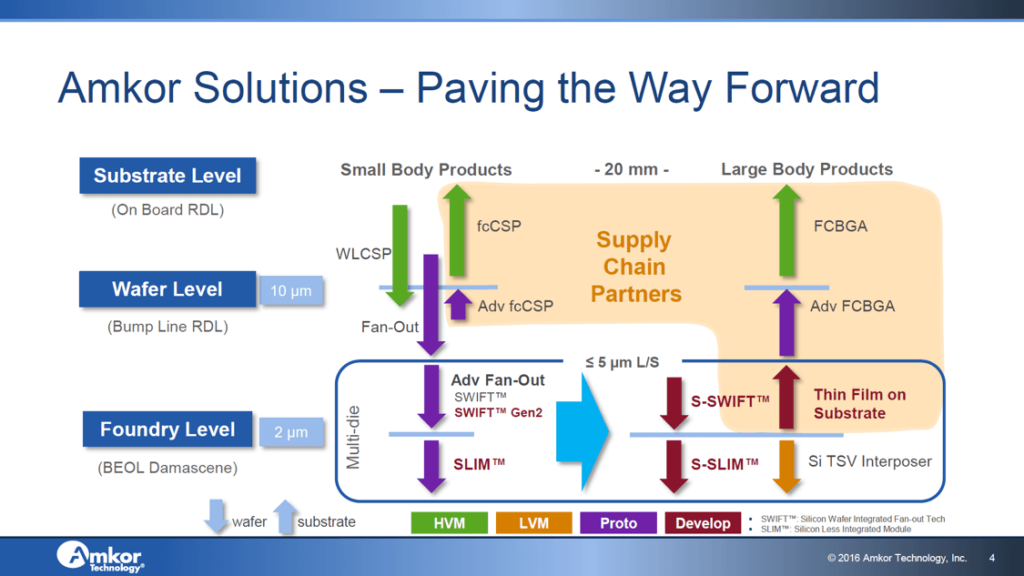
Mike Kelly presented a very good overview of Amkor’s current capabilities and plans. Figure 4 shows how multi-faceted today’s IC packaging requirements are and how much room for further innovation advanced packaging technologies offer. FYI, Amkor and Cadence announced in May 2016, that they are working together on a “Package Assembly Design Kit” for Amkor’s SLIM and SWIFT packages, to enable die-package co-design. This will make it easier for designers to meet performance and cost goals with Amkor’s wafer-level packages.
SPIL, now part of the same corporate umbrella as ASE, was represented by Albert Lan. He focused on outlining the importance of fan-out wafer level packaging (FOWLP) for mobile and wearable applications. Lan contrasted high-performance versus wearable packaging requirement, outlined SPIL’s manufacturing flows and explained why panel-level processing of these packages will become the most cost-effective manufacturing technology.
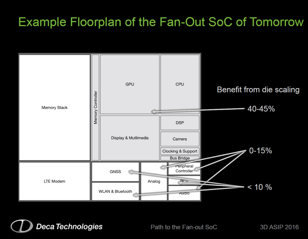
After enjoying Prof. Iyer’s CHIPS message, I was very glad to see that Deca Technologies is developing manufacturing processes to quickly and accurate place heterogeneous dielets in close proximity to each other on interposers. Tim Olsen explained how multi-die FOWLP – assembled with Deca’s processes, will enable system-level integration in thin and cost-effective FOWLP.
Figure 5 shows how Deca expects to enable side-by-side integration of dies. It also points out that different functions may benefit from scaling at very different rates.
So far I have only covered a fraction of all the interesting and useful messages conveyed at 3D ASIP 2016. Considering that this blog is already getting too long, here are quick summaries of other groups of presentations:
Digital cameras for smartphone and feature phones are the highest volume application for 3D ICs, serving as backlit image sensors. ams, Forza Silicon, ON Semi/Aptina, Raytheon, SMIC and SONY shared their accomplishments in this space.
Yole confirmed that memory cubes comprising vertically stacked dies are now the most widely used die-level IP building blocks. Tezzaron described their 4th generation memory cubes. eSilicon presented their design service capabilities and mentioned that they have already implemented more than half a dozen customer designs with HBM cubes on different interposers.
Boeing, Northrop Grumman and Teledyne, vendors to the military and aerospace segment, described how they used multi-die ICs and compound semiconductors to meet very stringent requirements.
Professors from UCSB and Ohio State talked about their research in multi-die IC technologies.
Atotech, AMAT, Besi, Corning, Brewer Science, EV Group, Samtech, SPTS, Suss MicroTec and Unimicron presented their equipment or materials capabilities and described how they contribute to the success of multi-die ICs.
Last, but certainly not least, this 3D ASIP conference also offered two tutorials. Qualcomm’s Beth Keser shared her vast expertise in FOWLP with a large audience. Prof. Bruce Kim from the City University of New York presented Electrical Modeling and Test Strategies for 3D Packages to a much smaller group, which I joined. This is another data point demonstrating the imbalance between manufacturing and design, we need to work on for 3D ASIP 2017.
Special thanks to iMAPS, who took over management of this conference from RTI, the technical organizers and session chairs of this important and informative conference. Learn more about it at http://3dasip.org/. Here’s to success in 2017. ~ Herb


Herb :
Excellent Summary, keep it up !
Dev