The Silicon Desert
Mar 30, 2026 · By Isabel Volpe · 3D In-Depth, R&D and Collaboration


Company to share key developments and highlights at SEMICON West
CMP/CMC/MOSIS announced a Grenoble-France based partnership for a 3D-IC multi-project wafer (MPW) service based on Tezzaron’s SuperContact technology and...
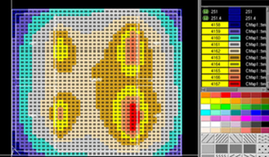
French research insitute, CEA-Leti and Docea Power, developers of software for power and thermal analysis at the architectural level,...