


Survey and Review of 2.5D and 3D IC Packaging Technologies
On April 9, 2014 Herb Reiter presented a 2.5D and 3D IC packaging-centric update in context with an IEEE/CPMT dinner meeting at the Biltmore Hotel in Santa Clara. About 50 silicon-, packaging-, assembly and test experts attended this 1-hour presentation. Most of them stayed for the very interactive Q &...

Will the Internet of Things Change the Way We Look at 2.5D and 3D ICs?
Years ago I saw Dr. Wayne Dyer on Public Television. He talked about “The Power of Intention”. The engineering-driven half of my mind didn’t pay much attention to such a mushy topic…. until Dr. Dyer confused me with what sounded like a play on words. He said “When you change...
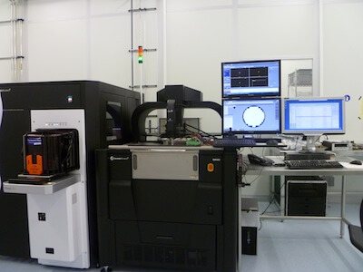
NORDSON Dage: XM8000 Wafer X-ray Metrology Platform
Fully automatic, in-line X-ray metrology platform for the measurement and defect capture of both optically hidden and visible features in wafers and 2.5D/3D IC packages. Available measurements include voiding, via fill, overlay and critical dimensions in TSVs, wafer bumps and MEMS. Testimonial: The XM8000 Wafer Metrology Platform provides a new...

ECTC 2014: A Preview of 2.5D and 3D Activities
Each year, the agenda of Electronic Components Technologies Conference (ECTC), an international conference sponsored by the IEEE Components, Packaging, and Manufacturing Technology Society (CPMT), is jam-packed full of tutorials, keynotes, panels, technology sessions, and interactive poster sessions covering the latest developments and emerging technologies in microelectronics components and packaging. Featuring the...

An Open Letter to Chip and System-level Designers Regarding 3D Integration
Dear Chip and System-level Designers, Allow me to introduce myself. My name is Françoise von Trapp, and I am known in the semiconductor industry as “The Queen of 3D”. This is because I have held a deep interest in 3D integration technologies, and have devoted the past 7+ years to...
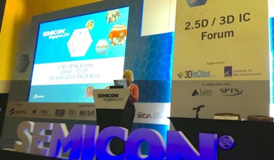
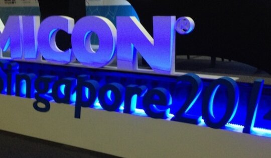
SEMI 3D IC Standards Workshop at SEMICON Singapore 2014
SEMICON Singapore 2014 featured a Friday round-table workshop about SEMI 3D IC Standards, which was held to determine local needs for standardization for 3D integration activities, to channel that activity to the right standards organizations. The goal was to trigger a discussion around what the most important standards are for...
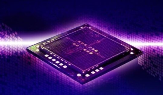
Process Improvements Target 3D IC Cost of Ownership
Customers have asked and suppliers are listening. One sign of progress from last year to this year at SEMICON Singapore’s 3D IC Forum was the number of supplier presentations focused on process improvements that have been developed to lower the 3D IC cost of ownership (CoO). In addition to the...
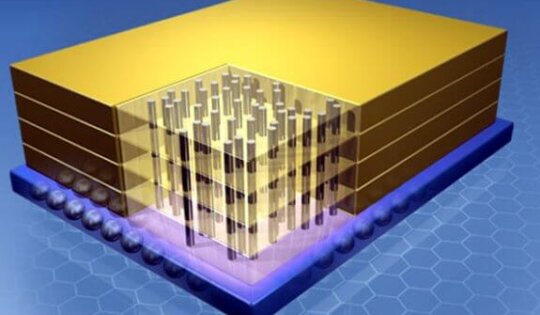
Circumventing Temporary Bond/Debond, and other Cost-Saving Approaches to 2.5D Interposers
While GLOBALFOUNDRIES and STATS ChipPAC may have it all figured out, there are many who still consider temporary bond/debond (TB/DB) to be an unsolvable challenge that adds unnecessary cost. The solution? Find a way to do away with it altogether. During the 3D IC Forum at SEMICON Singapore, both A*STAR...
3D IC Adoption: What’s it going to Take?
If, as we heard at last week’s 3D IC Forum at SEMICON Singapore, that technology challenges and cost are no longer keeping 3D ICs from volume manufacturing, and indeed the key players are ready to go, then what’s it going to take to get this 3D IC adoption party started?...
SEMICON Singapore 2014: A Rosy Outlook for 2.5D and 3D ICs
This week, at the invitation of SEMI Southeast Asia, I made the monumental trek from Phoenix, AZ to Singapore to attend SEMICON Singapore. While I know many of my industry colleagues make these journeys in the regular course of business, this was a new experience for me and my first...

2013 ITRS Roadmap Calls for 3D Power Scaling; Monolithic 3D Gains Traction
At the beginning of April, the Semiconductor Industry Association released the 2013 International Roadmap for Semiconductors (ITRS), which has traditionally served as a guide for “assessing and improving the future of semiconductor technology,” according to Brian Toohey, president and CEO, Semiconductor Industry Association. Sponsored by five regions of the world...

A Sneak Peek at IITC and AMC 2014
The recent announcement of the International Interconnect Technology Conference (IITC), combined with the Advanced Metallization Conference (AMC) in the Double Tree Hotel in San Jose, from May 20-23, caught my eye, because it also offers several sessions relevant for 3D-IC materials and manufacturing. On Tuesday, May 20, will be a...
Rudolph Technologies: JetStep S Series Lithography System
As advanced packaging facilities transition their manufacturing from round wafers to square panels, the JetStep S Series Lithography System is fully capable of handling panels up to Gen 3.5 (720x650mm). The system offers high throughput through a large printable exposure and increased productivity through on-the-fly autofocus for thick photoresists. Testimonial...

GSA Silicon Summit: What’s next for the 2.5D/3D Ecosystem?
Due to schedule conflicts, I was unable to attend this year’s Silicon Summit, which took place April 10, 2014 at the Computer History Museum, and featured a segment titled GSA Silicon Summit 2014: 2.5D/3D Ecosystem – What’s Next? Luckily, Rick McClellen, director of business development at Ziptronix briefed me on...
ASE and Inotera Memories to Offer Novel 2.5D Manufacturing Solutions
Last week, ASE and Inotera Memories announced they had entered into a joint development project (JDP) intended to both strengthen ASE’s system-in-package (SiP) capabilities and expand Inotera’s foundry services beyond its core competency of memory manufacturing to silicon interposers. The goal is to provide novel 2.5D manufacturing solutions. Prior to...

Oerlikon Systems: Pragmatic and Poised for 3D IC High Volume Manufacturing
In the last 40 years, the Principality of Liechtenstein has evolved from a purely agricultural state into one of the most highly industrialized countries in the world. But some how it has managed to keep its Alpine charm. That’s why at first glance, the city of Balzers, complete with its...

When You Come to a Fork In the Road, Take It
When Yogi Berra made this very wise statement, he certainly didn’t mean to give specific advice what to choose. I interpret his statement as an encouragement to make an educated decision and pick the best alternative, whenever you come to a fork in the road. The semiconductor industry is facing...
Cascade Microtech: In the imec 3D Test Lab
My visit to imec to meet with the Cascade Micorotech and imec 3D Test collaboration team included a tour of the 3D test lab to see the CM300 in action, so we suited up for Class 1000 cleanroom and stepped inside. Generally we would have had to prep for class...

Cascade Microtech Breaks Through the Barriers of 3D Test
For quite some time, the lack of cost-effective test solutions for 2.5D interposers and 3D stacked ICs (3D SICs) has been at the top of many industry experts’ laundry list of ‘what’s-holding-up-commercialization for 3D’. First, there are technology issues: fine-pitch probing, pin count, contact force and the phenomenon of weak...
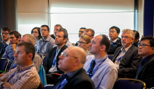
3D Workshop Panel Discussion Focuses on 3D Standards and EDA Tool Readiness
Are slow standardization and CAD-tool development hindering the progress of 3D IC design and integration? This was the topic of discussion during the Friday 3D Workshop at DATE 2014, which took place this year in Dresden, March 28, 2014. I was invited to moderate this panel discussion, which featured panelists from...