

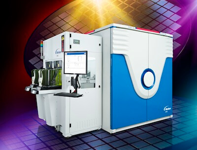
 Fully automatic, in-line X-ray metrology platform for the measurement and defect capture of both optically hidden and visible features in wafers and 2.5D/3D IC packages. Available measurements include voiding, via fill, overlay and critical dimensions in TSVs, wafer bumps and MEMS.
Testimonial:
The XM8000 Wafer Metrology Platform provides a new and unique X-ray metrology platform for fast, automatic and non-destructive measurement and defect identification on-wafer, and in-package (2.5D/3D), of the otherwise invisible defects, which can be created during the manufacturing processes used in TSV, wafer bump and IC packaging production, particularly the level and location of voiding. As such, it enables fast and realistic levels of extensive measurement coverage across each wafer or package at the magnifications necessary to give the best statistical analysis for the smallest TSVs and bumps used today. By providing unprecedented levels of precision, detection, automation and throughput, the XM8000 gives more and higher quality data than is possible with existing available systems.
- Nordson DAGE Website
- Date this Product was Introduced to the market: 6/24/2013
- Category Product is being Nominated for: Inspection/Metrology Tools
- Technical Information for the XM8000 X-Ray Metrology Platform


