
By Till Dreier and Julius Hållstedt, Excillum
Complex architectures with intricate interconnects, stacked dies, and buried features – the recent developments in advanced packaging come with great possibilities but also challenges. From off-line Failure Analysis (FA) to at- and in-line inspection in manufacturing — more efficient and higher resolution methods are needed to accelerate development and improve yield. X-ray nano-computed tomography (nano-CT) addresses this challenge by offering 3D imaging for e.g. Failure Analysis with sub-micron resolution, enabling precise visualization of internal structures such as micro-bumps, TSVs, bond lines, and voids.
X-ray Nano-CT
In our previous article, we examined the factors influencing measurement performance and provided best practices for optimizing X-ray imaging setups. In addition to introducing resolution, we discussed how to measure what parameters affect it. We also discussed key parameters of the X-ray system that can be optimized to achieve higher resolution and shorter measurement times.
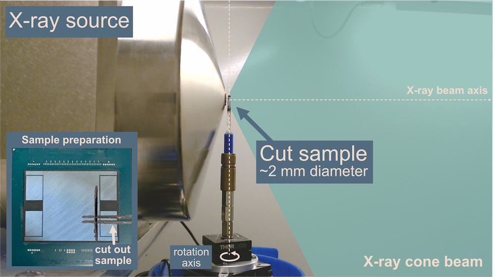
A key aspect is the optimization of the measurement geometry and to optimize magnification and number of X-ray photons per area. Hence, samples must be positioned as close to the X-ray source as possible. However, this often requires reducing the sample size to allow rotation in front of the X-ray source.
Figure 1 illustrates a typical experimental setup where a cut-out part of a processor, approx. 2 mm wide, is positioned close to the Excillum Nanotube N3 X-ray source, while still allowing it to rotate 360°. More details on the setup can be found in References [2] and [3].
A fundamental constraint in imaging systems is the diffraction limit, which defines the smallest distance between two objects that can still be resolved as separate entities. As objects are moved closer together, there is a point beyond where the imaging system can no longer distinguish them individually — they appear merged, as schematically illustrated in Figure 2.
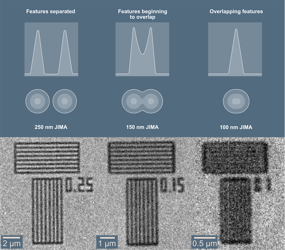
Bottom: As practical example of this effect X-ray images of JIMA test structures was acquired using a 300 nm X-ray spot. For 0.25 µm the features are fully separated, for 0.15 µm features are still resolved but with some overlap whereas for 0.1 µm the lines can no longer be resolved. (Note that different magnifications are used).
In the lower part of Figure 2, three examples are shown: 250, 150 and 100 nm imaged with a 300 nm X-ray spot, where features as small as 150 nm are resolved, whereas 100 nm features can be detected but it is not possible to separate the individual lines and spaces.
This illustrates the resolution limit caused by the size of the X-ray spot – as a rule of thumb, the achievable resolution is about ½ of the size of the X-ray spot. Resolution and advantages of different types of detectors are discussed further in References [2] and [4].
In the following section we will discuss how this performance and resolution can be used for real case advanced packaging case studies.
Imaging of micro-bumps using Nano-CT
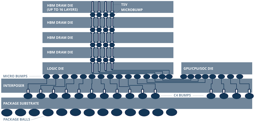
High Bandwidth Memory (HBM) is a critical enabler for high end systems offering ultra-fast data transfer rates and reduced power consumption through its 3D-stacked DRAM architecture. An advanced package featuring an HBM stack is schematically visualized in Figure 3. At the heart of this performance leap lies an array of micro-bumps—micron-scale solder interconnects that connect stacked dies with through-silicon vias (TSVs) to the logic die and subsequently to the interposer.
Due to their extremely small size, dense layout, and buried position within the stack, HBM micro-bumps present a significant metrology and inspection challenge. Traditional inspection and metrology tools often lack the resolution, penetration, or non-destructive capabilities required to thoroughly evaluate their quality and reliability.
With recent advancements in critical components in X-ray setups such as X-ray source, detectors and software, we will show some examples of both short measurement times as well as very high resolution. It should be noted that nano-CT of advanced packages normally involves sample preparation to allow for rotation of the sample close to the source. This sample preparation can in most cases be performed with very simple methods like sawing out a few millimeters of sample, as shown in Figure 1.
Since there is a tradeoff between speed, resolution and signal-to-noise, the first example illustrates 3D X-ray measurements of HBM micro-bumps performed in seconds. In the second example we will then go through how an increased measurement time can provide deep insights to variety of defects of the micro-bumps. While third example illustrates even higher resolution that can be achieved by increasing the magnification and extending measurement time further.

Fast overview scan – 30 s scan time
A fast (30 s) scan at 2.6 µm voxel size was used to provide an overview of the structures in the full sample, as shown in Figure 4. This voxel size enables an X-ray source spot size with high total power high X-ray flux which shortens measurement time. The resolution obtained from the reconstruction of this fast measurement is sufficient for navigation and a first assessment of the general structure of the sample from RDLs and vias in the substrate and interposer to the intricate micro-bumps of the HBM stack. This means that e.g. bump identification, alignment and finding missing bumps is possible. In addition, it provides a good overview for selection of a region of interest (ROI), as indicated by the red area in Figure 4, for high-resolution scanning.
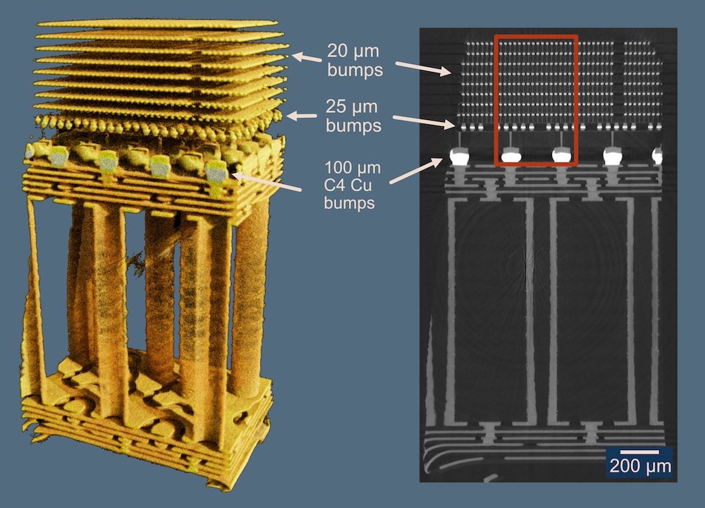
Figure 4: Fast overview scan. 3D render (left) and virtual slice (right) also illustrating the selected ROI for higher resolution investigation.
High resolution scan – 75 min scan time
For the high-resolution scan of the ROI (a small area centered on the DRAM modules), a voxel size of 600 nm was used providing data quality sufficient for analysis of the bump bonds with sub-micron resolution. Figure 5 shows the scanned region containing 100 µm C4 bumps at the bottom, 25 µm bump bonds connecting the logic die to the interposer, and 20 µm bump bonds connecting the DRAM modules. In the zoom-in, individual voids can be identified inside the 20 µm micro-bumps and the 5 µm TSVs can be visualized. Furthermore, the data quality enables statistical analysis of the micro-bumps and voids, by performing a segmentation of the bump bonds and their voids individually. A more detailed analysis of this scan and the 30 s overview scan has been published in [5].
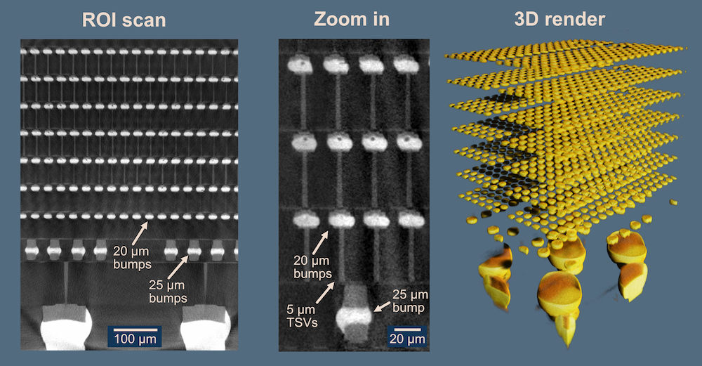
Figure 5: High resolution ROI scan providing details of TSVs, contact pads and micro-bumps including sub-micron voids.
High resolution scan – 6.25 h scan time
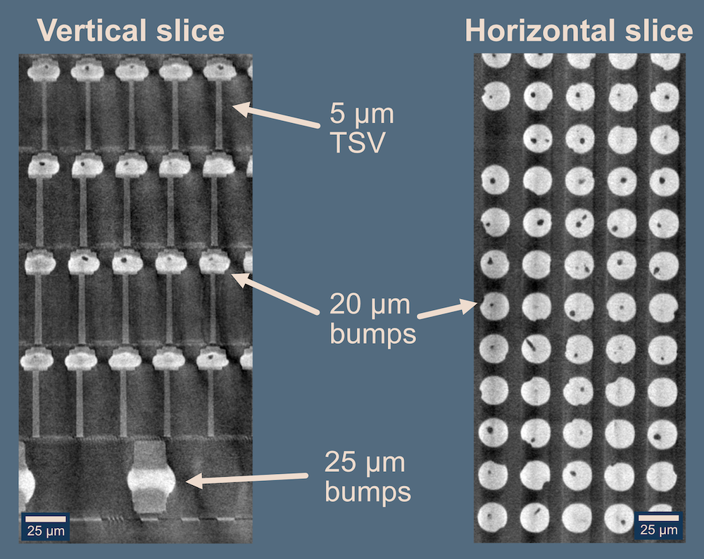
Further improving the resolution and data quality requires longer measurement time as smaller X-ray source spot size mean a lower power of the source, and increasing magnification requires the detector to be positioned further away. For this experiment, a 500 nm X-ray source spot was used with just over six hours scan time and a resulting voxel size of 400 nm. With this measurement, the internal structures of TSVs, contact pads, and micro bumps are clearly visible, as shown in Figure 6. This illustrates the usefulness of 3D X-ray imaging for imaging of small structures at very high resolution.
Imaging of hybrid bonding using Nano-CT
Hybrid bonding, also known as hybrid copper bonding, is a technique for interconnecting vias without solder. This method is illustrated in Figure 7, where small copper pillars are used to directly connect silicon dies. This approach is highly attractive from a cost perspective, as it can reduce the number of processing steps, e.g. the need to use a reflow oven to melt the solder for bump bonds. More importantly, it enables significantly higher via densities by allowing for smaller vias and tighter pitches, making it a key technology for next-generation 3D integration.
Although hybrid bonding has reached commercial deployment, several challenges remain — particularly improving yield, reliability, and overall competitiveness. As a result, there is a strong need for effective tools for failure analysis and process control to support continued development and scaling of this technology.

As hybrid bonds and connected TSVs are typically much smaller than the vias and micro-bumps in the previous sections, this naturally pose a significant challenge on 3D X-ray measurements. Here we performed a 6 h scan of the hybrid bonds inside an AMD Ryzen 7 5800X3D processor at a 300 nm voxel size illustrated in Figure 8. From individual 2D X-ray images these structures can only be seen from the correct angle, when unobstructed, as shown in the 2D projection image in Figure 8. In the reconstructed virtual slices using nano-CT, the hybrid bonds can however be seen much more clearly. The 3D reconstruction also highlights how small these structures are compared to the layers in the PCB and the 80 µm bump bonds. The hybrid bonds imaged here have a diameter of 1.5 µm, are 15 µm long, and arranged with a pitch of 9 µm, where not all possible locations are connected, indicated by the unconnected bonding structures in the virtual slice and 3D renders in Figure 8.
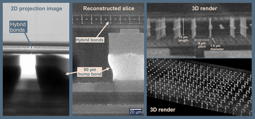
Figure 8: Imaging of hybrid bonds inside an AMD Ryzen 7 5800X3D processor, from a single 2D projection image to reconstructed virtual slice and 3D renders of the hybrid bonding structures.
Conclusions
In this article, we demonstrated the capabilities of high-resolution nano-CT in addressing critical challenges in advanced packaging, including the inspection of micro-bumps, hybrid bonds, and TSV structures. Our results highlight how optimized scanning setups requiring minimal sample preparation, enable both rapid and detailed analysis. This significantly accelerates failure analysis workflows while maintaining flexibility between ultra-high resolution and high-throughput imaging. Nano-CT thus emerges as a powerful tool to support quality assurance and innovation in complex semiconductor integration.
References
| [1] | T. Dreier and J. Hållstedt, “Unlocking the Mystery of X-Ray Imaging for Electronics and Semiconductor Inspection,” 3D inCites, 23 April 2025. [Online]. Available: https://www.3dincites.com/2025/04/unlocking-the-mystery-of-x-ray-imaging-for-electronics-and-semiconductor-inspection/. [Accessed 24 April 2025]. |
| [2] | T. Dreier, D. Nilsson, J. Hållstedt and J. Wittborn, “X-ray nano-tomography enabling sub-micron resolution failure analysis for advanced packaging,” in International Symposium for Testing and Failure Analysis (ISTFA), San Diego, California, USA, 2024. |
| [3] | T. Dreier, R. Krüger, G. Bernström, K. Tran-Lundmark, I. Gonçalves and M. Bech, “Laboratory x-ray nano-computed tomography for biomedical research,” Jorunal of Instrumentation, vol. 19, no. 10, p. P10021, 2024. |
| [4] | T. Dreier, D. Nilsson, J. Hållstedt and S. Hu, “Improved resolution in advanced packaging metrology through advanced nano-focus X-ray sources,” in 25th International Conference on Electronic Packaging Technology (ICEPT), Tianjin, China, 2024. |
| [5] | T. Dreier, D. Nilsson and J. Hållstedt, “Fast and high-resolution X-ray nano tomography for failure analysis in advanced packaging,” Microelectronics Reliability, vol. 168, p. 115694, 2025. |


