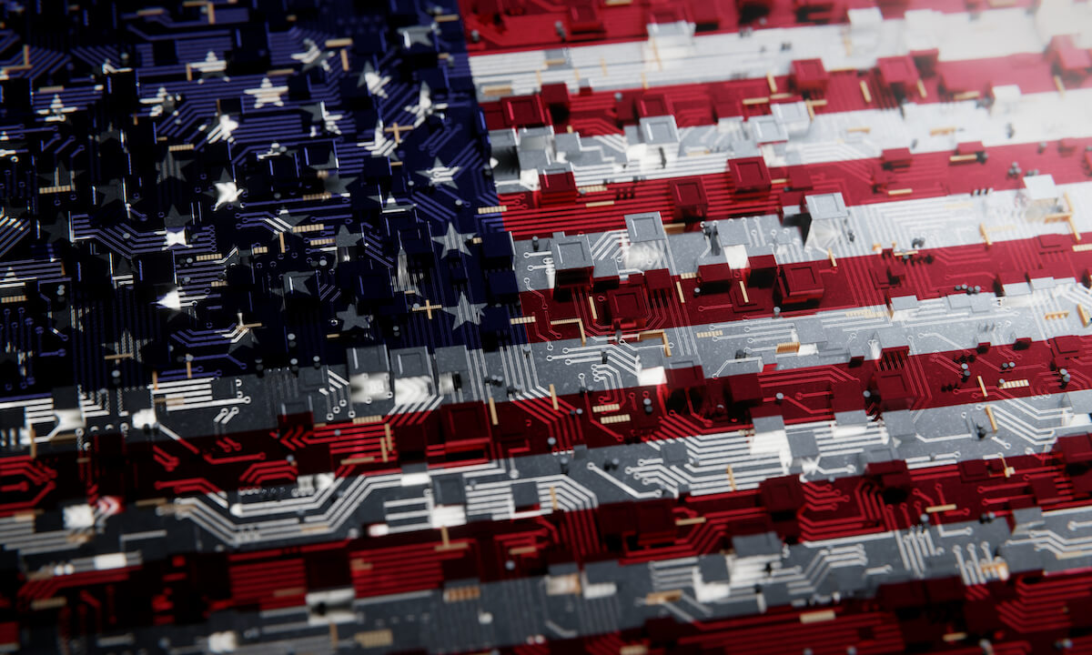
In IFTLE 534 we discussed the DARPA Next Generation Microelectronics Manufacturing (NGMM) program which will attempt to establish a domestic center for producing silicon/non-silicon 3D heterogeneously integrated (3DHI) prototypes. In IFTLE 535 we discussed the upcoming US Semiconductor Fab resurgence, which will generate the need for more on-shore advanced packaging. Now let’s take a look at a few other government-sponsored advanced packaging programs that are announced or underway.
SHIP Advanced Packaging Program
If you attended this year’s IMAPS Device Packaging Conference or IEEE ECTC, you became aware of the government-sponsored advanced packaging program known as the SHIP program. (Ed. note: Or of the recent IMAPS International Symposium – but more on that in later posts)
The State-of-the-Art Heterogeneous Integrated Packaging (SHIP) Program was developed to provide a sustainable access model for advanced packaging (AP) for the DoD. SHIP leverages cutting-edge commercial practices from industry leaders to address the gaps in DoD’s access to state-of-the-art (SOTA) microelectronics packaging within the domestic AP ecosystem. The SHIP Program is divided into two main projects: SHIP RF & SHIP Digital, headed up by Intel and Qorvo respectively.
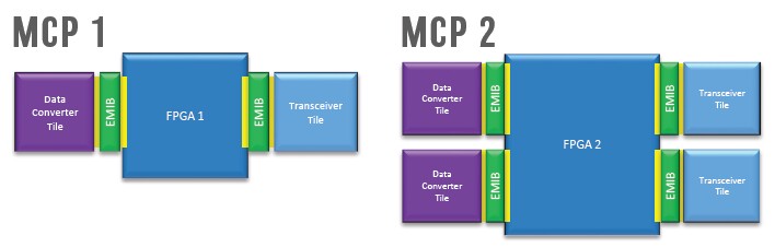
SHIP Digital is focused on developing state-of-the-art (SOTA) multi-chip packages to drive size, weight, power, and cost reductions and expand DoD access to chiplet-based MCP solutions. The program provides access to Intel’s SOTA microelectronics capabilities and leverages the reuse of chiplets including field-programmable gate arrays (FPGAs), custom application-specific integrated circuits (ASICs), data converters, transceivers, and optical tiles, among other technologies.
Intel has worked closely with the Defense Industrial Base to create two custom MCPs that will transition into fielded DoD systems. The MCP topologies integrate a data converter chiplet, FPGA die, and high-speed transceiver chiplet through the embedded multi-die interconnect bridge (EMIB) platform. MCP 2 increases the size of the package by doubling the tiles used; consequently, the input/output channels are doubled, and a more advanced FPGA is used to drive down power consumption and continue to increase size, weight, and power (SWAP) savings.
MCP 1 and MCP 2 are being commercialized as Intel standard parts and will be made available in 2023. DIB partners are encouraged to engage with Intel for specific customer needs or technical documents for use of one of the prototypes under development.
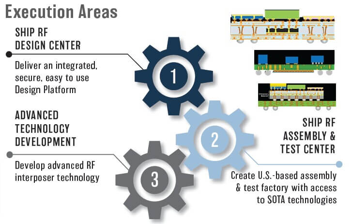
SHIP RF will establish domestic manufacturing for SHIP for RF applications, providing secure access to AP design, assembly, and test for DoD, DIB, and commercial companies, as well as supporting other DIB collaborators. SHIP RF has three execution areas: Design Center (DC), Assembly and Test Center (ATC), and Advanced Technology Development. Qorvo is enabling access to advanced RF packages by developing design kits, maturing AP platforms, and offering a selection of material choices to support specific use cases through SHIP RF DC and SHIP RF ATC.
Build Back Better Regional Winner
On Sept 2nd it was announced that the “Building Central Florida’s Semiconductor Cluster for Broad-Based Prosperity, led by the Osceola County Board of County Commissioners” was one of the 21 winners of the U.S. Department of Commerce’s Economic Development Regional Challenge and have been awarded $50MM in grants to boost the semiconductor industry in central Florida.
This funding is expected to accelerate the growth of the specialized semiconductor cluster at NeoCITY, a technology park developed in partnership with the state of Florida. Details of their proposal can be seen here.
The seven projects to be funded are shown below:
- Expansion of the fab
- Construction of connecting roads
- Advanced Packaging
- Digital Twin
- Upskill workforce development
- Cluster management org
- Governance and outreach
The advanced packaging processes focused at the center for innovation are unique because it focuses on manufacturing low volume highly customized chips that are demanded by the aerospace defense and medical industries. 97% of advanced packaged chips are made in Asia. The advanced packaging program led by Bridg will purchase and install advanced packaging equipment and stand up the new production line.
CHIPS Act Disbursement
The U.S. Department of Commerce recently outlined how it and other government agencies will disburse $50 billion from the CHIPS Act to chipmakers and other semiconductor-related groups. More detailed funding documents are expected by early February.
Around $28 billion, or nearly two-thirds of the total funding, will support Intel, Micron Technology, and other companies that make leading-edge logic and memory chips. Another $10 billion will help fund new manufacturing capacity for mature and current-generation chips, as well as specialty technologies like silicon carbide. An additional $11 billion is earmarked for the creation of a National Semiconductor Technology Center (NSTC), as well as an advanced chip packaging program and up to three new manufacturing institutes.
The CHIPS Program, under NIST and the DoD, aims to rebuild the U.S. semiconductor ecosystem while creating lucrative jobs domestically and strengthening national security.
The U.S. is expected to announce restrictions that would deny CHIPS funding to chipmakers investing in China, as well as foundries like TSMC and Samsung conducting production for Chinese chip designers at the 7-nm node and below. Both TSMC and Samsung have announced investments in the U.S. on the expectation of receiving CHIPS funding.
For all the latest in Advanced Packaging stay linked to IFTLE…………………