DARPA often selects its research efforts through the Broad Agency Announcement (BAA) process. The Microsystems Technology Office (MTO) at DARPA is currently seeking proposals “…to inform planning for the Next Generation Microelectronics Manufacturing (NGMM) program”. NGMM in a subsequent solicitation will attempt to establish a domestic center for producing silicon / non-silicon 3D heterogeneously integrated (3DHI) prototypes) by defining exemplar 3DHI microsystems and identifying the equipment, process, and facility requirements for manufacturing these microsystems. Proposed research should investigate innovative design and packaging of heterogeneous chip and wafer stacked components that enable advances in science and technology for 3DHI manufacturing.
In this solicitation, 3DHI refers to “…the stacking of separately manufactured components from different material systems, within a single package, to produce a microsystem that provides revolutionary improvements in functionality and performance”.
Expecting the next major wave of microelectronics innovation will come from the integration of heterogeneous materials, devices, and circuits through advanced packaging, DARPA is proposing to stand up a national accelerator for next-generation 3DHI. This national accelerator will take the form of a pilot-line manufacturing capability that would allow users from across the country to test their R&D designs without the need for investments in their own capability. This would be distinguished from the other congressionally authorized packaging efforts by its emphasis on the heterogeneous integration of multiple material systems, rather than prioritizing only silicon-based technologies.
This would become part of a multifaceted approach to strengthen US microelectronics industrial base as shown in Figure 1.
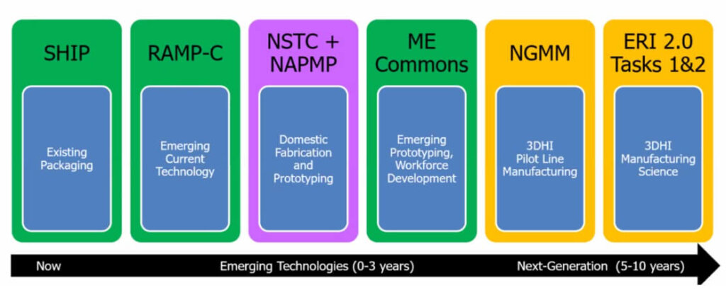
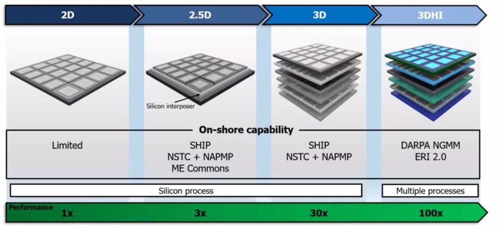
Figure 2 below describes how they see “on-shore capability” expanding as we implement these programs.
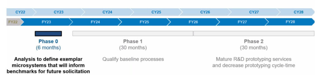
At the Aug 17th NGMM Proposer’s Day, MTO announced that the overall NGMM objective consists of 3 phases (Figure 3):
- Phase 0 (6 months): Analysis that defines:
- Exemplar 3DHI microsystems and
- Capabilities (i.e., process modules) are required. Proposals are due Sept 21, 2022.
- Phase 1 (30 months): Qualify baseline processes
- Phase 2 (30 months): Mature R&D prototyping services and decrease prototyping cycle-time
Phase 0 will be supported by $20MM. The Government will send out notification letters November, 2022 and expect contracts to be negotiated and initiated by February 2023.
Establishing the prototyping center is not being solicited within this BAA.
Foreign participants may participate “…to the extent allowed by applicable security regulations, export control laws, NDA’s, etc.”
A Phase 0 proposal should consist of a detailed report of exemplar 3DHI microsystems that could be fabricated in the 3DHI manufacturing center. In addition to providing a description of the layout, performance benefits, and applications, the report will describe the required equipment and process modules for manufacturing and testing the 3DHI microsystem.
![[err-ad-fallback-title]](http://www.3dincites.com/wp-content/plugins/a3-lazy-load/assets/images/lazy_placeholder.gif)
The input from Phase 0 will be used to create a separate solicitation for Phases 1 and 2 of NGMM. Phases 1 and 2 will focus on establishing the 3DHI manufacturing center, creating and finalizing baseline process modules, qualifying the pilot-line manufacturing process, and implementing the R&D access model for the center.
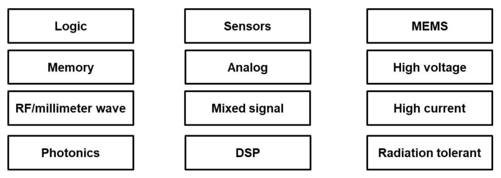
The exemplar microsystem should incorporate at least two building blocks from Figure 4.
The exemplar microsystems should have a minimum of three individual 2D chips vertically integrated together. In addition, they should contain a minimum of two disparate semiconductor material systems, such as Si, SiGe, GaAs, GaN, InP, HgCdTe, SiC, etc., rather than just two different Si CMOS technology nodes (e.g. 7 nm and 22 nm).
Proposers should address any needs for interface standards for chips that originate in different facilities and contain different semiconductors, metals, and dielectrics.
A detailed, step-by-step process flow is not expected for this research study. However, the report should encompass high-level capabilities and novel manufacturing approaches in the following areas: through substrate vias, bump and bond pad formation, redistribution layers, wafer/chip/die bonding, backside processing (including wafer/die thinning), reconstituted wafers, dicing, and die attach. In addition, a description of the required tests, metrology, and reliability toolsets should be provided. The analysis should identify the key equipment necessary for accomplishing these processes, including an assessment of equipment availability.
A complete description of the program can be found here.
For all the latest on Advanced Packaging stay linked to IFTLE………………