
Leading-edge semiconductor fabs haven’t been built in the U.S. for a while but that’s about to change. Let’s look at how and where those changes will take place. It is certainly worth reviewing such information because these fabs will be driving the matching advanced packaging that will also be installed on shore. If there is anything that IFTLE is sure about it is that the US government now understands that it does us no good to manufacture 5nm chips in the US if we then have to ship them to Asia to get them packaged.
Well, when it comes to microelectronics take it from your elders like IFTLE, “this is the dawning of the age of IC packaging”. If you are a packaging engineer, the world is about to really open up for you as “onshoring” puts your skill set in high demand. In the next year or two — as the US government begins dispensing financial support like COVID shots — if you cannot find a great job, i.e the job you always wanted, well maybe you’re in the wrong profession!
According to the semiconductor industry association (SIA), the U.S. share of semiconductor manufacturing decreased from 37% in 1990 to 12% in 2021, and even more importantly, as of 2019, 100% of the world’s most advanced logic semiconductors (< 10nm) were produced overseas.
Politicians have finally realized that the reduction in manufacturing capability poses a major threat to America’s national security and to the overall economy. This, in turn, has generated calls to build state-of-the-art (SOTA) semiconductor fabs on shore.
In fact, in the last 12 months or so at least six major players in the Global Semiconductor industry ( GlobalFoundries, Intel, Micron, Samsung, Texas Instruments, and TSMC ) have all announced new semiconductor production facilities in the U.S., all of which, one can assume, will be partially financed by the now approved CHIPS legislation.
GlobalFoundries
In the summer of 2021, GlobalFoundries announced plans to invest $1 billion to increase Malta NY‘s Fab 8’s capacity from 47.5K to 60K wafer starts/month. Fab 8 processes wafers using FinFET-based nodes (14LPP, 14HP, 12LP, 12LP+) as well as non-volatile memory (NVM), RFSOI, and silicon photonics.
Along with the $1B investment in Fab 8, GF announced plans to fund a brand-new facility “through private and public partnerships.” GF says this new capacity will serve the growing demand for secure, feature-rich chips needed by high-growth markets, including automotive, 5G connectivity, and IoT.
Intel
Intel is investing $40B+ in four U.S. semiconductor fabs that are scheduled to come online over the next 3-5 years. Currently, Intel is reportedly building two chip production plants in Arizona and two in Ohio, and an advanced packaging facility in New Mexico.
Intel broke ground on Fab 52 and Fab 62 near Chandler, Arizona, in the fall of 2021. They will come online in 2024 at a projected cost of $20B. The fabs will use Intel’s 20A fabrication technology which includes gate-all-around field-effect transistors (GAAFETs) and PowerVia backside power delivery.
In Ohio, Intel has announced they will establish a mega production site that will house up to eight semiconductor manufacturing facilities (possibly an advanced packaging facility, too, but Intel has not confirmed this)(Figure 1).
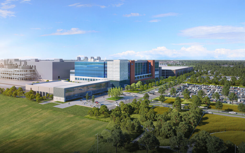
The site will require investments of ca. $100B over the next decade. Intel’s Ohio campus will require suppliers to also establish a local presence, which means a major expansion of the U.S. semiconductor supply chain since none of them now call Ohio home.
The first two semiconductor fabs near Columbus Ohio, will reportedly use Intel’s 18A/20A nodes when they come online in 2025. This project will initially cost over $20B. To support the development of the new site, Intel pledged an additional $100 million toward partnerships with educational institutions to build a pipeline of talent and bolster research programs in the region.
Intel is also investing $3.5B in its advanced packaging facility in Rio Rancho New Mexico which becomes operational in 2023 – 2024 and will enable the fabrication of complicated multi-chiplet designs in the coming years. The Rio Rancho site will enable advanced packaging technologies like EMIB and Foveros.
Micron
Micron, the globally 3rd ranked memory chip vendor, announced plans to invest approximately $15 billion to construct a new fab for leading-edge memory manufacturing in Boise, Idaho. This will be the first new memory manufacturing fab built in the U.S. in 20 years. This is reported to be the first of Micron’s multiple planned U.S. investments following the passage of the CHIPS and Science Act. Micron has announced plans to invest $40 billion through the end of this decade to build leading-edge memory manufacturing in multiple phases in the US.
In late August it was learned that Micron has requested tax incentives to build a new semiconductor fab outside Austin TX.

The application describes a large semiconductor manufacturing facility to be built approximately 30 miles south of Austin in Lockhart TX. Reportedly the fab will be built in eight phases and could cost as much as $160 billion.
Samsung Foundry
Since 2009 the Samsung Foundry division has produced 32nm, 28nm, and 14nm SoCs in Austin, Texas. Samsung eventually moved its leading-edge node production to South Korea, leaving its S2 fab in Texas with older trailing nodes (14nm/11nm ~ 65nm). In late 2021 the company announced plans to build an all-new fab near Taylor, Texas. After reviewing multiple US locations Taylor was chosen based on the local semiconductor ecosystem and the proximity to Samsung’s current manufacturing site in Austin, allowing the two locations to share the necessary infrastructure and resources. The company indicated that it would use the facility to manufacture chips for 5G, mobile, high-performance computing (HPC), and artificial intelligence (AI) applications starting in the second half of 2024.
The project will cost $17 billion, and the new facility is scheduled to come online in the second half of 2024.
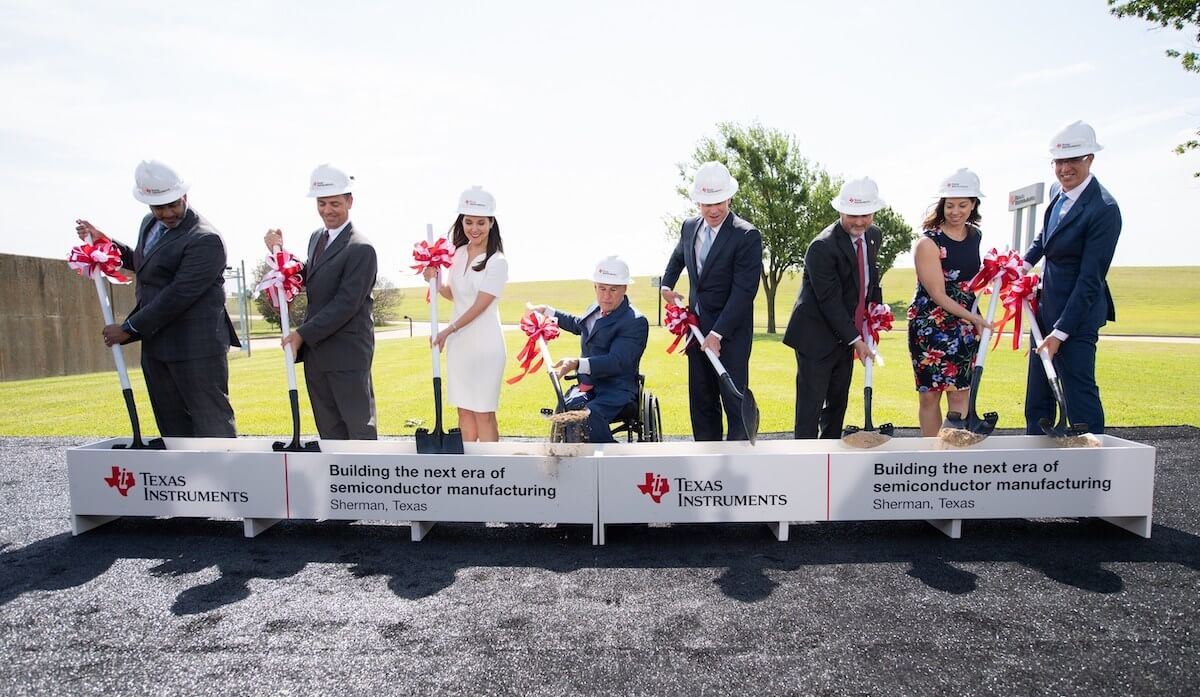
Texas Instruments
Texas Instruments is the world’s largest manufacturer of analog chips. TI is building a $30B fab near Sherman, Texas. The new site will be built in four phases, with the first fab coming online in 2025.
The company currently has three 300-mm semiconductor production facilities in the state (DMOS6 in Dallas, RFab Phase 1 in Richardson, and the soon-to-be-completed RFab Phase 2 in Richardson), so it can share engineering talent between the sites.
TSMC
In late 2020 TSMC announced plans to build a $12B, 5nm fab with 20K wafers/month capacity near Phoenix AZ. Production at the facility is to start in 2024. US companies reportedly account for 62% of TSMC sales. The Arizona facility will reportedly make chips for Apple iPhones and Mac computers.
According to Nikkei Asia, TSMC plans to expand the plant’s capacity to 120,000 units per month. Rumors from Taipei are that TSMC plans on phasing up to 6 fabs in this area producing chips using TSMC’s N5 (N5, N5P, N4, N4P, N4X) family of process technologies.
The Taipei Times is reporting (via Nikkei Japan) that TSMC is also considering building an advanced IC packaging facility in the US in response to the US desire to bring more of the tech supply chain onto the US mainland.
Tom’s Hardware has recently taken a look at announced on-shore fabs for GlobalFoundries, Intel, Samsung, TSMC, and Texas Instruments. It’s a good read with further detail.
For all the latest on Advanced Packaging stay linked to IFTLE………………
Feature photo above: Texas Instruments Chairman, President, and CEO Rich Templeton (center); Texas Governor Greg Abbott; and Sherman Mayor David Plyler, along with company leaders, participate in a groundbreaking ceremony for TI’s new 300-mm semiconductor fabs in Sherman, Texas.


