
TSMC considers Packaging Facility in the US
The Taipei Times is reporting (via Nikkei Japan) that TSMC is considering building an advanced IC packaging facility in the US.
The potential US packaging plant would be equipped with the latest 3D stacking technologies. IC packaging is highly localized in Asia and is an area where Washington has stated the need for onshore capability.
TSMC currently operates advanced IC packaging and testing plants in Taoyuan, Hsinchu, Taichung, and Tainan in Taiwan. TSMC is building an advanced IC packaging facility in Miaoli County, where it is to start production next year for clients including Advanced Micro Devices Inc. and Google.
TSMC last year announced that it would invest US$12 billion to establish a 5nm, 20K wafers/month facility in Arizona. According to Nikkei Asia, TSMC is planning to expand the plant’s capacity to 120,000 units per month. Production at the facility is to start in 2024.
TSMC is considering a US packaging facility in response to “Washington’s desire to bring more of the tech supply chain onto the US mainland. The US is heavily dependent on chips from Taiwan, raising concerns over supply chain risks. The US reportedly accounts for 62 percent of TSMC sales. The Arizona facility will reportedly make chips for Apple iPhones and Mac computers.
EMIB Technology Advances at ECTC 2021
Let’s begin our look at the presentations at ECTC 2021 with the session on 2D and 3D Chiplet Interconnects in fan-out wafer-level packaging/panel-level packaging (FO-WLP/PLP) that focused on the use of EMIB interconnect.
Intel
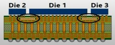
Gang Duan of Intel presented “Die embedding challenges for EMIB Adv Packaging Technology”. Recall EMIB uses small silicon interconnects embedded in a laminate for high-density connections between chips or chiplets as shown in Figure 1.
At Intel, EMIB is reportedly being widely adopted in FPGA, high-end graphic processor units (GPU), artificial intelligence (AI), server, and other data-centric high-performance computing (HPC) segments.
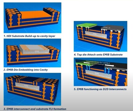
By leveraging panel-level high-density interconnect (HDI) substrate build-up processes, the EMIB bridge interconnect is embedded into a cavity followed by encapsulation and first-level interconnection by forming vias (laser or lithography) to the bridge pads. Heterogeneous dies or chiplets are then attached by thermocompression bonding as shown in the figure below. The Intel STRATIX 10 FPGA is being manufactured using EMIB 55µm pitch technology. Embedding bridged dies accurately and reliably inside the organic substrate is key to the EMIB technology.
Die embedding challenges:
One must minimize bridge die warpage and bridge die shift and control die coplanarity during bonding. Die shift during encapsulation is known to be a high-risk factor during fan-out wafer-level packaging. For EMIB, films are used for encapsulation. The author notes that there are significant restrictions on EMIB die movement and die shift. In order to achieve continued technology scaling high accuracy embedding is clearly required. As IFTLE has noted for several years, this is not a trivial process and will be beyond the capability of most practitioners, i.e not for the faint of heart.

Duan reports that Intel has achieved modules with 10+ embedded bridge die.
ASE
Lihong Cao of ASE – Austin TX discussed “Advanced HDFO Packaging Solutions for Chiplet Integration in HPC Applications.”
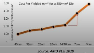
In her introduction, Cao points out that the cost per mm sq of a 7nm, 250mm sq die is about 4x that of a 45nm die and 5X for a 5nm die. This led to a discussion about the use of disintegration and the use of chiplets to fabricate today’s/tomorrow’s modular systems.
It still amazes IFTLE how this disintegration (also called disaggregation and/or the simple one-word “chiplets”) and its potential to increase performance and lower cost has in only a few years become accepted by the mainstream. When IFTLE talked about this technology 5+ years ago as AMD was first introducing it, it was considered shear heresy!
Cao then described three types of ASE fan-out chip on substrate technologies (FOCoS) : chips first; chips last and FO embedded silicon as shown in Figures 4a, b, and c.
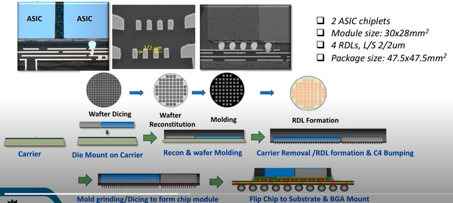
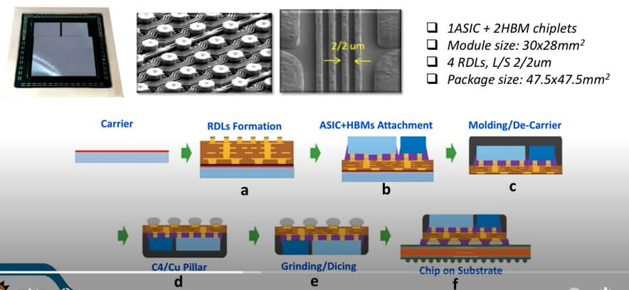
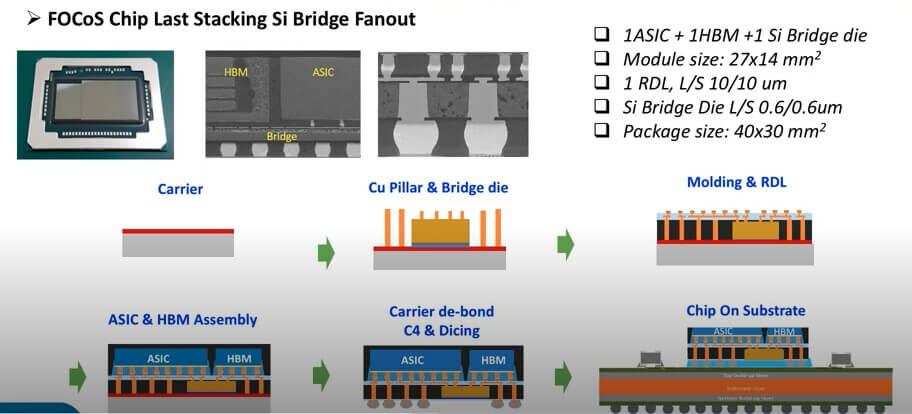
Warpage control is a major factor for these packages, which means the materials selections are important. Impact of die thickness, EMC, and Underfill choices are critical. Once optimized, all packages passed 1000 hours of high-temp storage (150°C); 264 hrs of HAST, and 1200 thermal cycles (-40–+125°C)
For all the latest in Advanced Packaging stay linked to IFTLE……………………………………….


