
Back from our IFTLE #500 trip down memory lane, let’s continue our look at the SEMI Heterogeneous Integration Summit. We’ll focus on the semiconductor supply chain, the advanced packaging market, and advancements in image sensor technology.
Semiconductor Supply Chain Research at BCG
Martin Schrems, senior advisor at Boston Consulting Group, gave a presentation on how heterogeneous integration (HI) is affecting semiconductor supply chain dynamics in the electronic market.
We are seeing front-end CMOS technologies applied to back-end packaging solutions. The slide below shows how technology has evolved over the past 20 years.
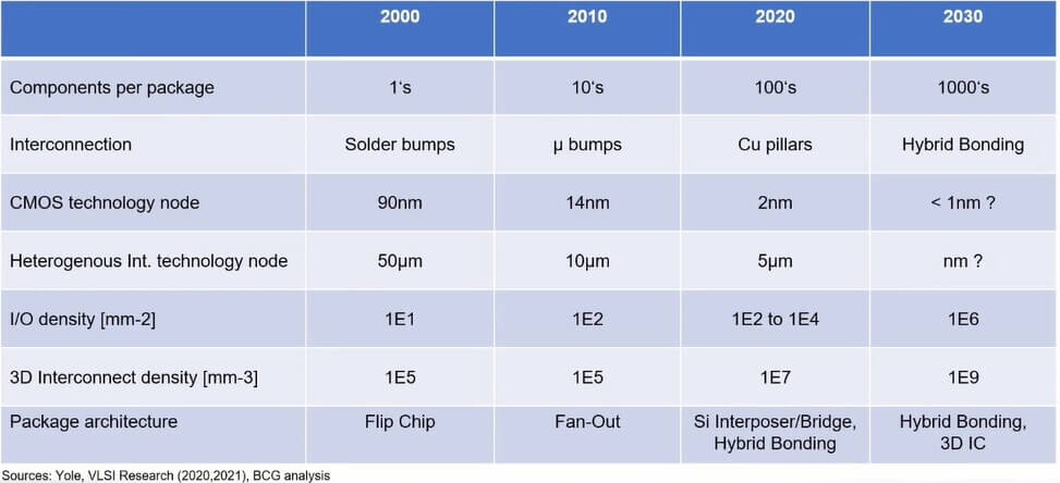
I have a few issues with this chart. I think 1000s of components in a module by 2030 is way too aggressive. CMOS technology node for 2020 is also not correct (aggressive) and the row titled HI technology node is a mystery to me??
BCG’s take on who is participating in value capture at the various levels of electronic systems (Figure 2).
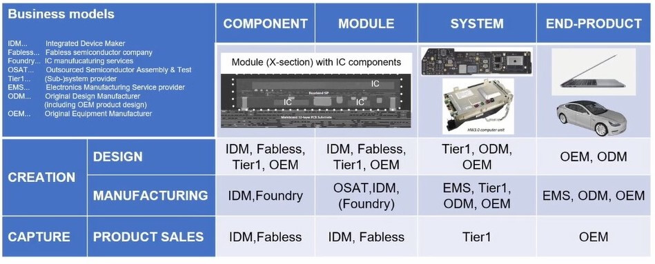
This looks at who creates the value in terms of design and manufacturing and who captures the value in terms of product sales. All of these actors are competing for the value in the system.
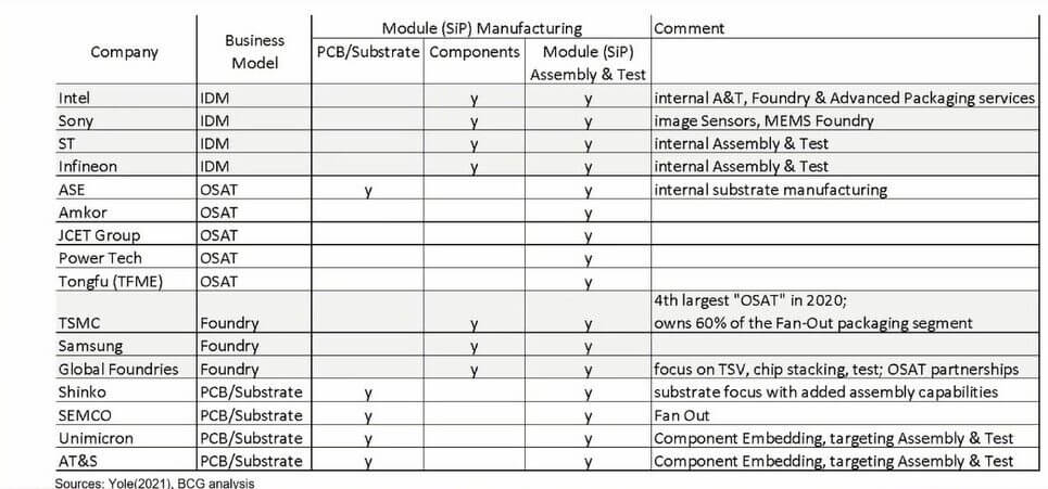
They see a convergence of EMS – board assembly with OSATS – packaging assembly.
IDM, OSAT, foundry, and substrate suppliers’ business models compete for system-in-package (SiP) module manufacturing value. In 2020, IDMs have ~25%. OSATS hold >60% dominant share. PCB/high-density laminate suppliers are trying to enter with embedded solutions. Foundry share is rapidly growing led by TSMC by using wafer level, fan out and chip stacking front end type technologies. With the foundries (TSMC, Samsung, GF) entering the market front-end and back-end technologies are merging. The foundries are in a strong position to take market share of this value. They are all looking to expand their advanced packaging capabilities causing a convergence of capabilities (Figure 3).
The same thing is happening on the design side of the semiconductor supply chain, where OEMs like Apple and Tesla are designing their own chips and boards and, in some cases, even looking to manufacture them.
Prismark Partners
Brandon Prior, of Prismark Partners, updated the company’s thoughts on the 3D and advanced packaging markets.
There continues to be a proliferation of new packaging designs and technologies. Most of the new technologies enable multi-die modules either side-by-side or 3D. While some may never reach HVM, many will. Basically, there needs to be a large enough end market for a given technology to ensure that the entire supply chain (materials, equipment, foundry, OSAT IDM, etc.) is willing to support and invest.
Recently there have been major investments in advanced packaging as shown in Figure 4.
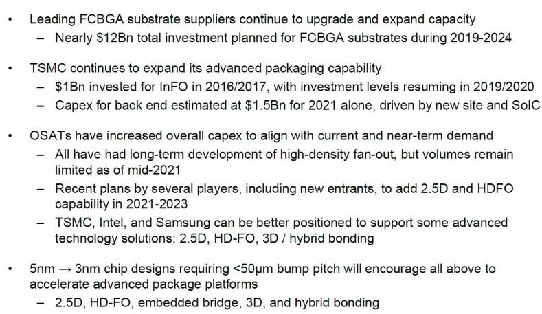
Sub-50µm bump pitch is driving advanced packaging.
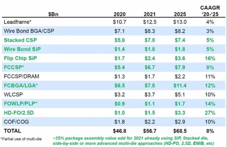
Nearly one-third of the IC package assembly value is already using advanced packaging (SiP, stacked die, side-by-side or advanced multi-die approaches) technologies (Figure 5, highlighted in green).
Prismark is also a believer in the migration from c4 bumping to hybrid bonding as shown in Figure 6:
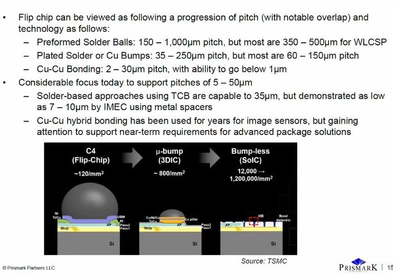
Prismark sees all major players are moving to hybrid bonding solutions in order the achieve the density requirements of the future.

Samsung – CIS Approaching human vision
Haechang Lee, VP of the Automotive sensors division, reports that the mobile image sensor market is growing to around $19B by 2025, and will account for about 75% of the total image sensor market. The automotive image sensor market will be growing at a much faster rate reaching 4.1B by 2025.
Today, auto camera resolution is about 1 MP, but in 2025 resolution will increase to 8 MP. Today’s vehicle has about three cameras which will increase to about five by 2025. Automotive technology will quickly migrate to applications such as drones and robots.
There is a drive to improve image quality such that CIS will emulate human vision more and more. It is hoped that this technology will augment human vision to make our lives better.
To emulate human vision CMOS Image sensor technology must achieve the following:
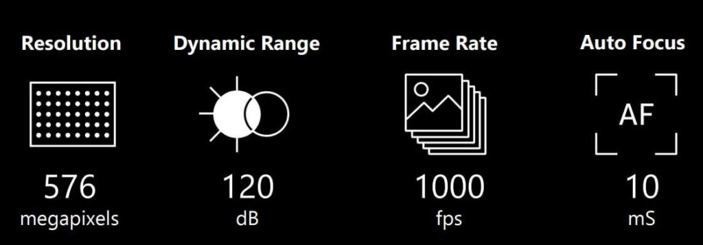
Over the last two decades, the aggressive scaling of pixels has enabled the following resolution improvements. Samsung expects resolution to approach 600 MP by 2025, which would match the resolution of the human eye.
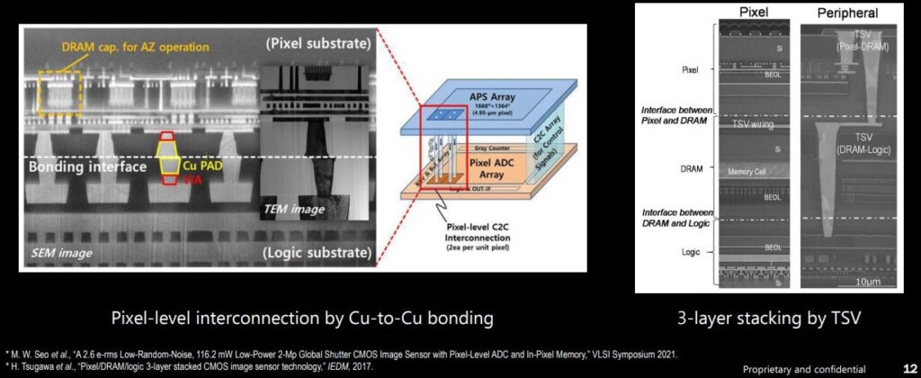
Key to high-performance sub-micron pixels is deep trench isolation (similar to deep trench capacitor technology) which reduces optical and electrical cross talk.
Today’s SOTA frame rate is about 120/sec. We can increase the frame rate severalfold using 3D integration, which improves the data throughput between stacked die.
A way to expand human vision capability is to go beyond the visible spectrum. Of special interest are the near-infrared (NIR) and short-wave infrared (SWIR) regions. Near IR can use silicon devices but SWIR requires compound semiconductors. SWIR can see through water ( i.e. rain and fog) and smoke.
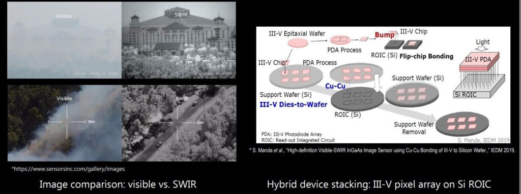
We will need new packaging solutions to integrate compound semiconductors with silicon, i.e heterogeneous integration.
For all the latest on Advanced Packaging stay linked to IFTLE……………………….


