


When people weren’t talking about the coronavirus at this year’s 2020 IMAPS Device Packaging Conference and its co-located Global Business Council, they were talking excitedly about the arrival of the golden age of packaging, heterogeneous integration, and most specifically, chiplet integration.
Keynote speakers (Doug Yu, TSMC; Christian Hoffman, Qualcomm Germany; Subu Iyer, UCLA; Rich Rice, ASE; Jan Vardaman, Techsearch International, Inc; Vaibhav Trivedi, Yole Developpement; Max Min, Samsung; and Wolfgang Sauter, Marvell;) and panelists (Robert Patti, NHanced Semiconductors, Inc.; Kevin Yee, Samsung; Paul Mescher, Microsoft; Jawad Nasrullah, zGlue; Ravi Mahajan, Intel Corp.) together built a solid case for chiplet integration in general, talked about the challenges it overcomes and offered updates on chiplet architectures that are either available now or in development.
We heard about the key drivers: 5G, AI engines, and Big Data, and edge computing, to name a few. We had history lessons about interconnecting transitions, and about how integration is transforming the world. We learned that the value proposition for chiplet integration is that it is a game-changer that will improve the cost of monolithic die, and we even engaged in controversial discussions about whether we should be calling them chiplets or dielets or even multi-chip modules (MCMs). We heard about Xperi’s hybrid bonding and its promise for 2.5D and 3D stacking to support chiplet integration.
Marvell’s Wolfgang Sauter actually counted how many times the words “integration”, “heterogeneous” and “chiplet” were uttered by other speakers: 46, 19, and 10 respectively. “It’s indicative of what’s going on in the industry,” he said.
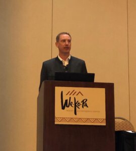
Sauter, who unfortunately drew the short straw for keynote timeslot on day three, delivered the most succinct and definitely the most entertaining talk of the week. A fixture at ECTC, this was his IMAPS Device Packaging Conference debut, and he did not disappoint. Not only did Sauter drive home some important points, but he also did a fine job of commenting on points from previous presentations and the panel discussion, which was aptly titled: Are Chiplets the Answer to HPC? So, I decided to frame this blog post around his comments, for those of you who didn’t get to hear what he had to say.
Get Moore out of the Package
Don’t you just love a play on words? This was the title of Sauter’s talk, and he meant it quite literally. “I don’t want to talk about Moore,” he said. What he wanted to talk about was advanced packaging.
Although he did talk a little bit about Moore’s Law. He actually touched on my favorite topic: How it’s not really a law at all. It’s an observation that’s not based on any science. Sauter shared a chart that plots the course of Moore’s Law over the past 50 years (Figure 1).
“Anything you can draw a straight line through over the course of 50 years is quite boring,” he said. “Does the straight line really matter?” Something to think about.
“A product is not just a chip,” Sauter added. “It’s more complicated than that. It’s a module you can plug into different systems and can be used in multiple places. A chip is not a product to me.” He went on to explain that different functions don’t really want to be on the same chip. It makes more sense to integrate chips based on different functions, such as I/O density, analog and RF content, and memory.
Sauter knows what he’s talking about. He spent 15 years at IBM in packaging development “without a clue of what it would be needed for.” Then he spent four years in product solutions at GlobalFoundries, where the chip people wanted to talk about what drives customer architectures (“I was the dumbest guy in the room for four years”) and one year at Avera Semi working on ASIC solutions. Now at Marvell working in Product Solutions, he’s come back full circle to packaging topics and chiplet technologies. It’s important to note that in these 20 or so years, Sauter didn’t actually change companies. The companies changed around him: GlobalFoundries acquired IBM Microelectronics, and spun out Avera Semi as an independent company, and then sold it to Marvell Semiconductor. This career has shaped his perspective on the importance of packaging.
Why 5G needs Chiplet Integration
A successful 5G infrastructure, noted Sauter, will work anywhere from Siberia to the Sahara. It also needs packages designed to deliver much more data than they currently do. “It’s enough data for me, but my daughter, who uses Snapchat, needs the next generation of data,” he joked. But he makes a good point. The millennials and future generations of adults consume and generate so much more data than past generations. It’s only going to increase, and we need an infrastructure to support it.
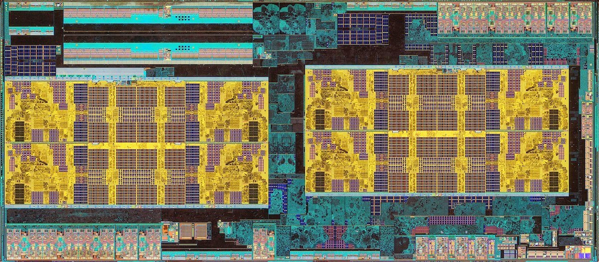
Meeting these needs requires different RF front end devices to be integrated into one system, and often goes beyond reticle size, calling for a different approach than the conventional system-on-chip (SoC) allows. The Marvell Falcon, for example, uses the chiplet approach to integrate beyond a reticle to deliver the needed performance. What we do for our kids!
From MCMs to Chiplet Integration
During the panel discussion, the argument about chiplet being just a new name for MCMs came up: If I didn’t work then, why do we think it is the solution now. This was not unlike the discussion of a few years ago about SiPs being a new name for MCMs. Quite frankly, I’m getting soooo tired of this argument.
The panelists agreed: while chiplets are essentially a form of MCMS, they have moved beyond what MCMs could do. Samsung’s Kevin Yee said chiplets are the evolution of MCM. zGlue’s Jawad Nasrullah noted that the differences are operational and commercial: Chiplet integration allows for multiple companies to provide the silicon and a third party can design and integrate it. Nhanced Semiconductor’s Bob Patti said chiplets and MCMs are part of a continuous spectrum, and he thinks the key difference has to do with I/O and partitioning. It’s about achieving interconnect density that can’t be done with organics or glass.
Sauter revisited the topic as well in his keynote and provided a concrete answer. “Is it new? It is absolutely not new,” said Sauter. “MCMs were launched in 2004 and weighed 5 lbs. IBM built the whole system end-to-end in-house. It disappeared and it’s coming back.”
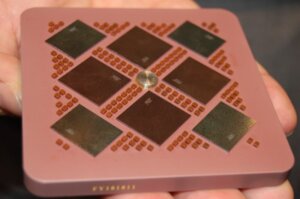
And therein lies the difference. Chiplets are not your father’s MCMs. They don’t weigh 5 lbs (Figure 2). They aren’t built using FR4, wire bonds, and ceramic packages. Since 2004, technologies have matured and evolved. Yesterday’s MCMs didn’t have silicon substrates, active interposers, the interconnect fabric or hardened IP to allow for mixing and matching functionalities into one system. They didn’t have processes like die-to-wafer hybrid bonding or through-silicon vias as interconnect options.
Today’s chiplets resemble yesterday’s MCMs in concept only. So, let’s move on. Let’s acknowledge the brilliant minds of the past who came up with a great idea before its time, and let’s be excited about what new opportunities chiplet integration will afford. ~ FvT


