Despite travel restrictions due to the Coronavirus, Dr. Douglas Yu, Vice President of R&D for TSMC gave a keynote via WebEx at the IMAPS Device Packaging Conference on March 3, 2020. He described the new era that the industry has entered, and specifically how heterogeneous integration technologies are ushering in Moore’s Law 2.0.
With continued demand to improve cost per function, the industry is migrating from IC scaling to system scaling. Dr. Yu explained the importance of heterogeneous integration in driving the cost per function down. As a comparison, SRAM scaling lasted 30 years and he described the SRAM and I/O trend and said that while we continue to increase transistor count over the years, improvement in power efficiency is also important. Gate count continues to increase.
Innovative packaging solutions are needed, and Dr. Yu provided examples of what companies including AMD, Cray, HP Enterprises and others are doing. He explained why wafer-level integration requires the seamless integration of IC and microsystems — both in the front-end (FE) and back-end(BE)) — and how leveraging the wafer fab for fine pitch systems along with Cu technology and tools with yield learning and quality control is a winner.
Dr. Yu referred to TSMC’s wafer-level system integration (WLSI) Platform circle drawing (Figure 1), which shows the integrated fan-out (InFO) mobile options. He said it is important to leverage TSMC’s Open Innovation Platform (OIP) ecosystem and supply chain.
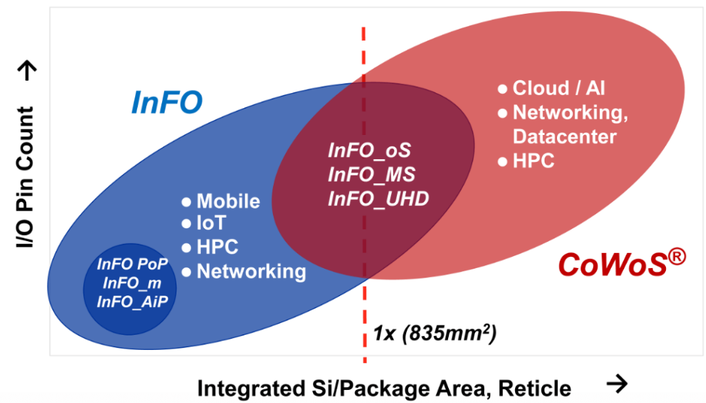
TSMC’s CoWoS has been in production since 2012. The largest example of CoWoS is a 2,460 sq. mm interposer (3X reticle, 4-mask stitched interposer), where two 600 sq. mm systems on chip (SoCs) and eight second-generation high bandwidth memory (HBM2) are mounted on the interposer. InFO_oS has been in production for networking since 2017. These packages are examples of TSMC’s back-end integration.
Changing the Game for Moore’s Law 2.0
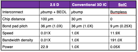
System on IC (SoIC™) is an example of front-end integration and Yu says that TSMC considers this technology to be a game-changer. Table 1 shows the advantages of SoIC™. There is virtually no distance between the integrated chips and a very small bond pad pitch is possible.
The interconnect density of a SoIC is 12,000 to 1,200,000/mm2. SoIC™ can be face-to-face (F2F) or face-to-back (F2B) and examples include chip-on-wafer (CoW) and wafer-on-wafer (WoW).
![[err-ad-fallback-title]](http://www.3dincites.com/wp-content/plugins/a3-lazy-load/assets/images/lazy_placeholder.gif)
Dr. Yu discussed the disruptive high integration of SoIC with CoWoS, InFO (FE 3D x BE 3D) to further enhance the power-performance-area-cost (PPAC) advantages for More Moore (MM) and More-Than-More (MTM). He explained that TSMC’s FE system integration approach unleashes architectural, integration, and design innovation. 3D system scaling can drive the cost-per-function for long-term semiconductor technology migration.
Dr. Yu concluded with the introduction of a new metric to calculate 3D interconnect density: number of lines and traces/mm across chip boundaries on an interposer, or substrate multiplied by the number of vertical interconnects (minimum pitch) between stacked chips/mm2. Another way to describe the metric is line density (horizontal) multiplied by area density (vertical). ~ J. Vardaman
For more on TSMCs SoIC, read Steffen Kröhnert’s recent post covering the 3D & Systems Summit in Dresden, where Dr. Yu also gave a keynote talk.