This week we continue our look presentations from SEMICON Europa’s Advanced Packaging Conference.
Intel’s Reliability Test
Beth Keser’s group at Intel Germany discussed their “product-on-board” reliability test for 0.3mm WLCSPs.
The existing JEDEC/IPC board-level methodology tests are fine for traditional packaging solutions for non-extreme low K dielectric (ELK) fab nodes. Future products require new methods of reliability testing for advanced silicon nodes and advanced packaging.
The IC shrinkage at front-end-of-line (FEOL), backend-of-line (BEOL), and assembly backend (BE), to increase the future functionality of mobile and automotive products, requires the usage of advanced semiconductor nodes and advanced materials. This makes reliability and robustness testing more important than before.
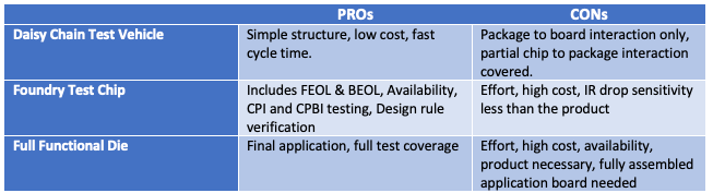
The various test vehicles used for board-level reliability test include:
- Daisy chain test vehicle concept
- The foundry test chip concept and
- The full functional die concept.
The pros and cons of each are shown in Table 1.
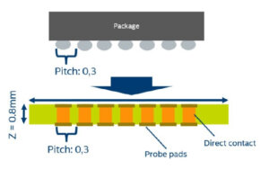
Intel’s new “product-on-board” test vehicle approach is a one-to-one vertical routing of all connections or by a redistribution layer (RDL) in the board stack-up, which enables enlargement of the pitch and the pad size on the bottom side of the board. The increase of the pitch and the pad size reduces the PCB costs and the number of measurement contact fails. Test board manufacturing can be completed in a standard substrate line. The assembly of the chip to the test board can be done in a standard flip-chip (FC) assembly or surface mounted technology (SMT) line. This is depicted in Figure 1.
The 3 failure modes found after testing include:
- RDL stack to the last metal pad of the chip resulting in white bumps
- UBM including RDL2 opening pad lift-off
- Crack propagation within the RDL
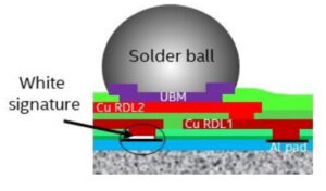
Failure mode 1
The main physical failure mode is delamination between the RDL stack via and backend-of-line Al pad. This can be detected by scanning acoustic microscopy (SAM) as a white signature. The x-section in the white spot area (Figure 2a) showed a gap/delamination between the RDL stack via and to the backend of the line Al pad (Figure 2b).

Failure mode 2
The second failure mode observed showed cracks within RDL 2 up to the first layer of the RDL stack, as detected by SAM.
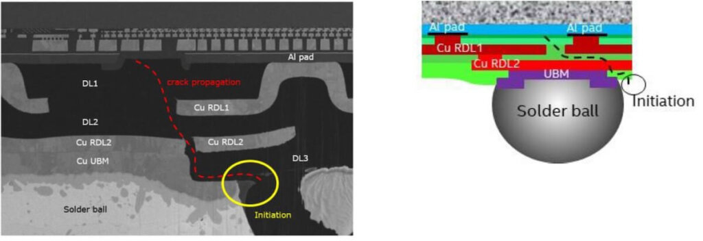
Failure mode 3
The third failure mode was a combination of Failure Mode 1 and Failure Mode 2. The crack propagated in some cases up to or in the BEOL area. The initiation points of the failure modes were at the corner of the solder ball and UBM interface.
They further conclude that their “product on board” test reveals the same failure mechanisms after stressing as the existing test methods.
Atotech Looks at Chemistry’s Role in Reliability
The Atotech presentation examined the role of chemistry in the reliability of packages composed of heterogeneous materials. Primarily a plating materials company, Atotech focused on issues concerning copper RDL trace requirements as we begin ramping 5G.

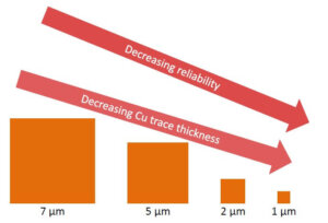
Miniaturization not only involves the decrease of trace width but also of trace thickness. As copper RDL traces get thinner they also get less reliable (Figure 4.)
From the stress vs. strain curves shown below for different copper thicknesses, we also see that the rupture of the copper lines is also dependent on the copper “purity” (although “medium” & “high” purity are not defined in these slides) (Figure 5).

This can be understood in terms of copper metallurgy. Upon annealing, copper impurities tend to accumulate in the grain boundaries, making these points of embrittlement, i.e decreasing the ductility and tensile strength.
One also needs to have smooth Cu surfaces to avoid the skin effect in upcoming high-frequency 5G applications. This is in contrast to a common way of achieving good copper adhesion to polymer dielectrics, which is to intentionally roughen the copper surface in the way they roughen PCB copper surfaces. Atotech proposes that new adhesion promoters will have to be found to eliminate this issue. [IFTLE adds “or better dielectrics with better adhesion.”]
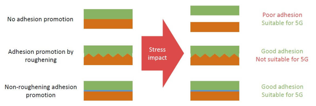
Lastly, Atotech recommends we assume good adhesion and look at the copper/dielectric structure as a composite. As can be seen in Figure 7, copper/PI composite is much more ductile than copper alone for thin copper structures.

In summary, the requirements include:
High copper purity
Smooth copper surfaces for 5G
Excellent adhesion to dielectric
For all the latest on Advanced Packaging stay linked to IFTLE…………………………