
Continuing our look at the 2019 SEMI 3D and Systems summit in Dresden, we look at presentations on advanced packaging platforms and hybrid bonding reliability.
Systems Plus
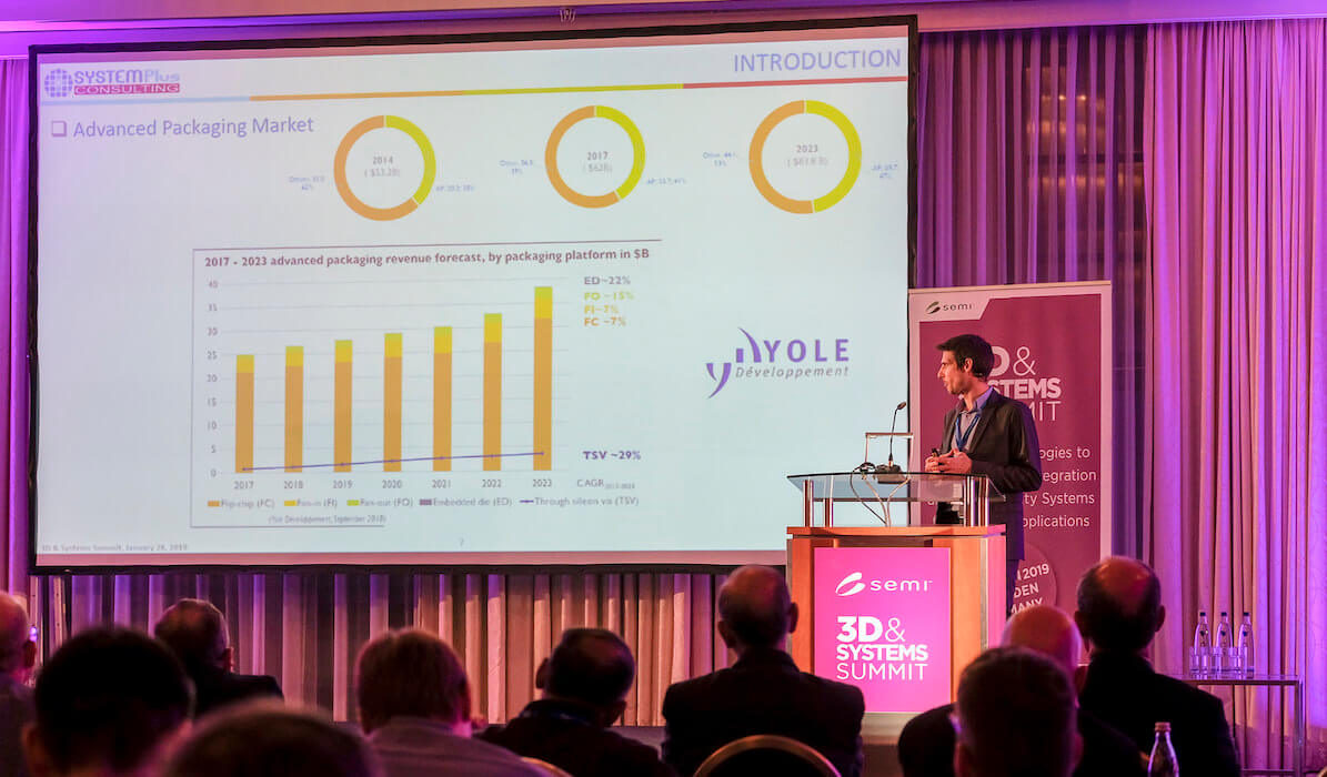
Romain Fraux of System Plus discussed their analysis of the latest advanced packaging platforms on the market. The Yole Développement quantitative analysis of the market is shown in Figure 1:

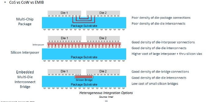
They offered the comparison slide shown below for chips connected on a substrate vs. Si interposer v.s Intel’s embedded multi-die interconnect bridge (EMIB):
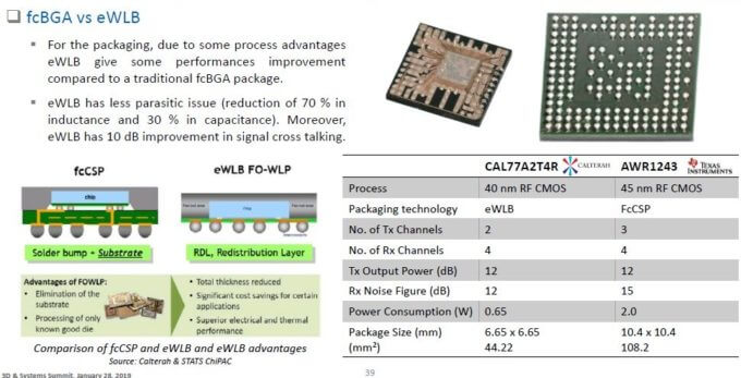
….and the following slide comparing a flip chip BGA to a fan-out WLP:
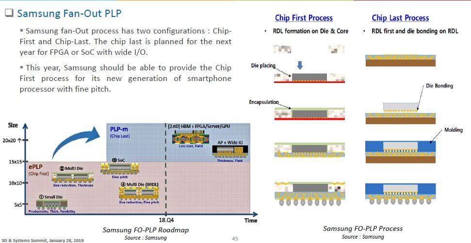
…and a comparison of chips first vs chips last Samsung panel level process FOWLP (Figure 3):
ST Micro – Crolles
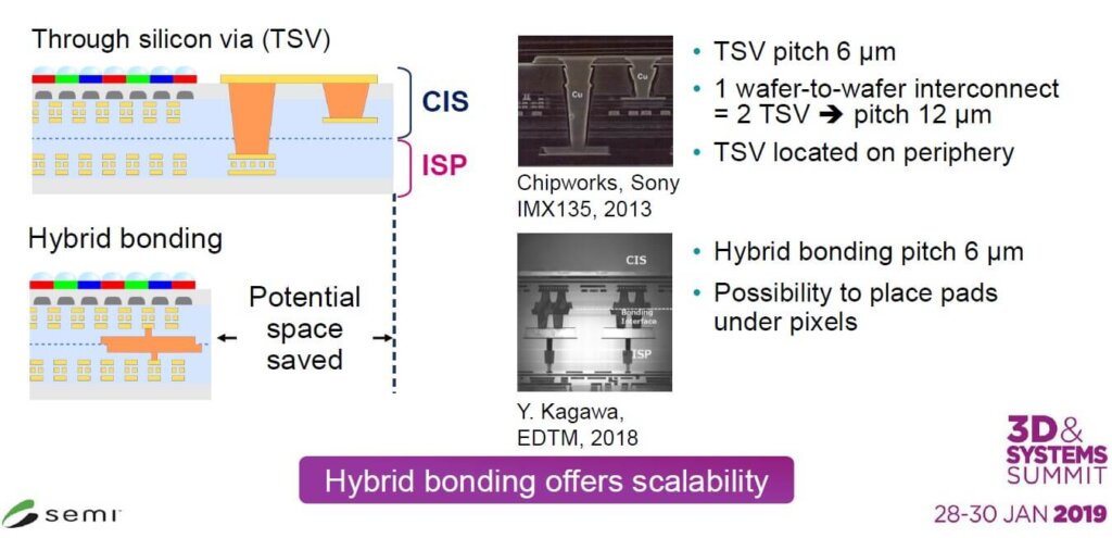
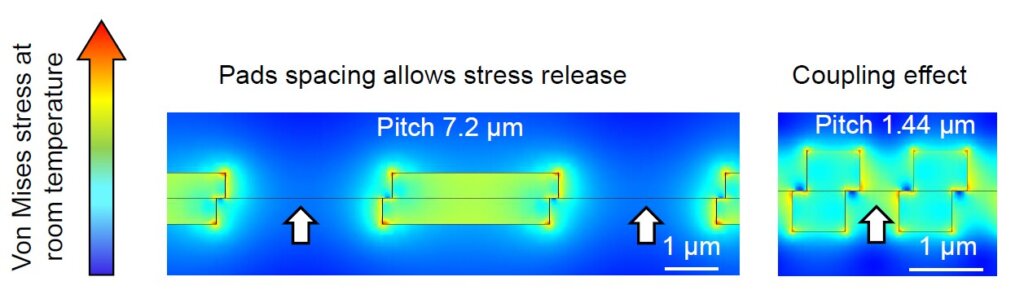
Joris Jourdan of ST Micro- Crolles discussed the reliability of fine pitch hybrid bonding interconnects. For devices like CMOS image sensors, hybrid bonding allows bonds to be under the pixels rather than occupy space on the periphery (Figure 4).
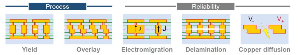
Key challenges for fine pitch hybrid bonding include:
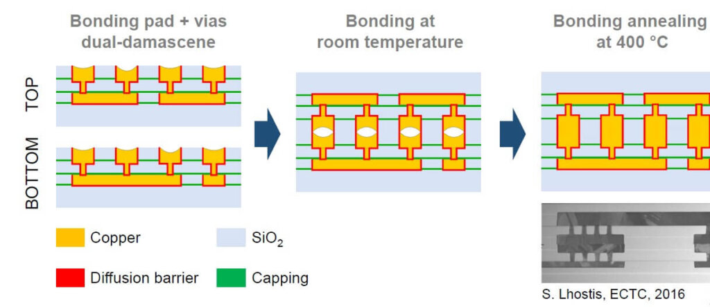
The hybrid bonding process flow is shown in Figure 7. ST Micro has validated it at a 7.2µm pitch.
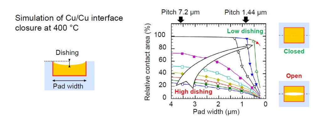
Smaller pads require significantly less dishing during the CMP process as shown in Figure 8.
Simulation of residual stress after bonding annealing and cooling shows a higher likelihood of delamination for tighter pitches.

STM concludes that do not limit electromigration lifetime is limited by BEoL performance and that the bonding interconnects do not limit electromigration lifetime.
TSMC
Digitimes reports that TSMC Advanced packaging will generate nearly $3 billion in revenues in 2019 according to TSMC Chairman Mark Liu.
TSMC is slated to apply its 4th generation CoWoS technology to package core HPC chips, networking chips and switch chips in 2019 and launch the 5th generation of the process in 2020.
TSMC is reportedly also set to begin production of SoIC (system-on-integrated chips) packaging technology in 2020. Based on 3D stacking concepts … “SoIC can integrate logic IC, memory, and chips fabricated on different process nodes such as 10nm I/O devices paired with 7nm core chips”. SoIC is more advanced than TSMC’s existing wafer-level packaging processes CoWoS and InFO.
Industry sources report to Digitimes that “…TSMC will keep pursuing more advanced and multi-function packaging technologies to help clients integrate heterogeneous chips and overcome the limits of Moore’s Law, i.e. chip scaling”.
For all the latest in Advanced Packaging stay linked to IFTLE………………….


