Heterogeneous integrated circuit (IC) packaging has made a full entrance into the high-performance computing arena. The target applications are broad, running the gamut from artificial intelligence (AI), deep learning, data center networking, supercomputers, and autonomous driving. In fact, a new generation of deep learning AI, leading central processing units (CPUs) for data center servers as well as new performance-leading CPUs for the latest blade servers have literally been made possible by these remarkable IC package constructions.
These cutting-edge technologies are leading the way for incredible advancements. Moreover, they all have a common characteristic: high-speed, high-performance ICs.
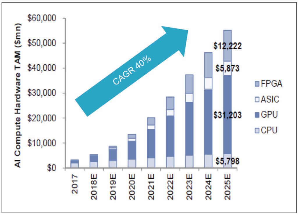
Investment agency Goldman Sachs Group has predicted that global AI hardware microchips including CPUs, graphics processing units (GPUs), application-specific integrated circuits (ASICs), field-programmable gate arrays (FPGAs) and others, will grow at an annual compound rate of more than 40% in the coming years (Figure 1).
In deep learning, continuous advancements in algorithms and big data accessibility combined with high-performance compute engines based on heterogeneous IC packaging are driving the giant leap forward for this technology wave. The package construction has permitted a two-fold leapfrog in what was possible previously, specifically: a memory bandwidth improvement thanks to high bandwidth memory (HBM) introduced by Samsung and Hynix, and the ability to provide more off-package signaling capacity.
Heterogeneous Packaging Approaches
FCBGA MCM
Heterogeneous digital integration using flip chip BGA (FCBGA) packages has been occurring for years and the variety of approaches has been nearly endless. The intra-die routing capability for multichip modules (MCMs) is good, and as long as the layer count to achieve this can be accommodated, it will continue to be a viable approach for many devices.
TSV
Through-silicon via (TSV) development took several years to perfect in silicon interposers but really ushered in the modern heterogeneous surge. The implications were profound, as the highest bandwidth DRAM (HBM) available were designed exclusively for silicon interposer applications. This new performance level was only available in 2.5D TSV packages: first in ultra-performance graphics, then deep-learning accelerators and now in data center networking switches and server CPUs. The main requirement for silicon interposers is that the HBM device uses an ultra-wide 1024-bit parallel bus requiring signal routing traces of 2µm width or smaller. This is 8-10 times the routing density of an FCBGA substrate.
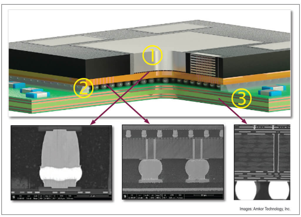
Amkor’s TSV reveal process and chip-on-wafer (CoW) packages have been in high-volume manufacturing (HVM) for three years. The assembly processes are high-yielding flagships of the new ultra-clean K5 facility in Song-Do, South Korea, near the Incheon International Airport. Figure 2 shows the key elements of a typical implementation of this packaging technology.
HBM: Just the Beginning
Processors used in conjunction with HBM in 2.5D TSV packaging constructions came first, but this is viewed as just the beginning. Today, the expense of 7nm and upcoming 5nm design will sharpen the focus for the content placed into the system-on-chip (SoC), ASIC or the processor. Leading advancements beyond single SoC approaches are in-package combinations of the processor and multiple discrete I/O die and even multiple processor chips in an effort to increase the core count and discrete I/O die. Several current examples of these have been prototyped and announced.
One of the key intersections between new levels of device performance and heterogeneous IC package structures is the intra-die signal routing capability. The 2.5D interposer offers a copper back-end dual-damascene technology with excellent fine-line capability and reasonable electrical signaling performance for short runs. Today, 2.5D TSV is the proven path for HBM integration into your product designs.

Another up and coming technology uses the so-called “dies-last,” high-density fan-out (HDFO) approach.
HDFO Packaging
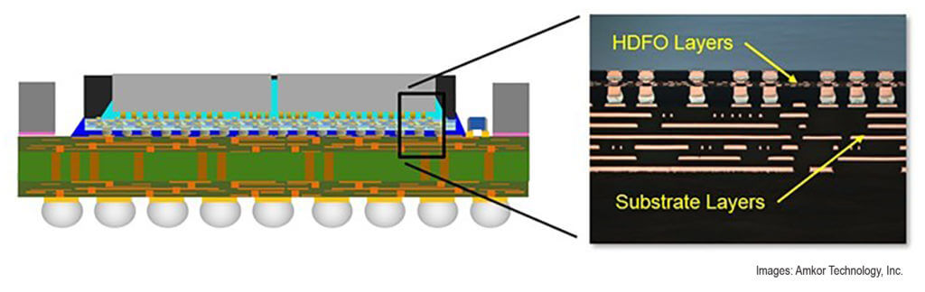
HDFO packaging is being developed as another crucial pillar for heterogeneous integrations to lower the cost of high-performance heterogeneous applications. This fine-line redistribution layer (RDL) approach is capable of 2µm line/space and 4-layer counts to provide the inter-die routing. In this case, the copper/organic dielectric RDL layers are fabricated on a glass or silicon carrier and then the wafer is populated with functional die and molded in a manner very similar to 2.5D designs (Figure 3).
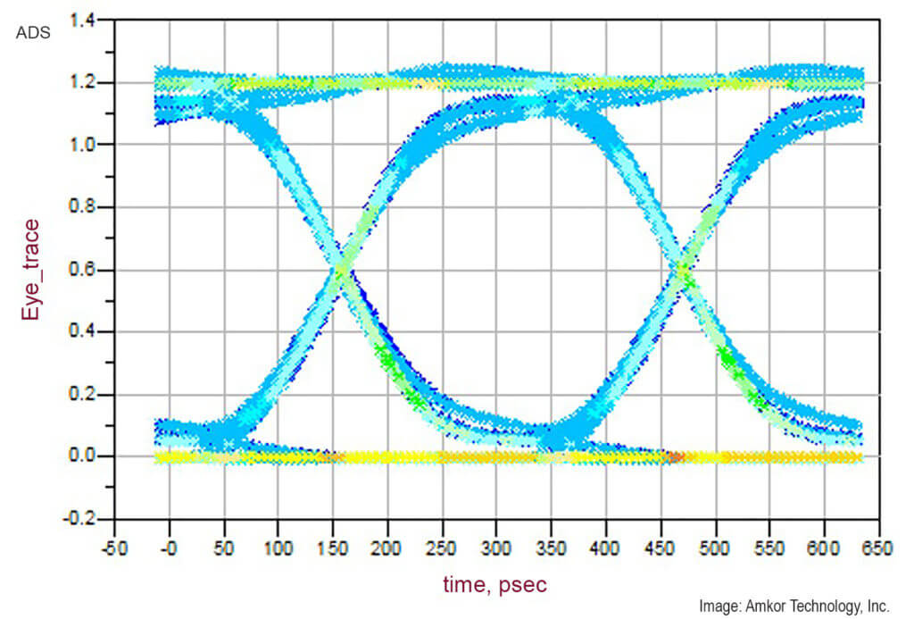
For the 2.5D package design plan, the design flow and design methodology are very different from traditional package designs. For example, an HBM2 DRAM having 4,000 bumps, and the main chip maybe having tens of thousands of bumps and multiple chips, are connected through an interposer. To do this, the design, simulation for optimization, and rule-checking need to advance. Addressing these challenges, Amkor has already developed outsourced semiconductor assembly and test (OSAT), industry-leading process assembly design kits (PADKs), and a design flow to achieve electronic design automation (EDA) connectivity with Cadence and Mentor Graphics.
The kits are introduced during the design stage and achieve asynchronous debugging design environment to carry out comparisons between schematic and layout diagrams and to perform all design rule checks (DRCs). This process achieves rigorous design verification and sign-off. In addition, by extracting the design, interposer and substrate models, and implementing co-design and co-simulation, design-for-performance (DFP), design-for-cost (DFC) and design-for-manufacturing (DFM), are also achieved. Figure 4 shows one example of a simulated eye-diagram, with the HBM data bus operating at 2 GHz frequency.
Summary
Heterogeneous packages have overcome the existing limitations of monolithic integration and significantly increased the capabilities and performance of today’s electronic products. As silicon integration faces additional and even more difficult challenges, the next step towards heterogeneous packaging will fulfill an even greater role to take end products to ever higher levels. The packaging solutions are available today to make the next generation products a reality.
Editor’s Note: This article by Ron Huemoeller, Mike Kelly, Curtis Zwenger, Dave Hiner, and George Scott, Amkor Technology, Inc. first appeared in 3D InCites: The First Decade. Download the issue here.