

Editor’s note: For several years now, Mentor Graphics has evangelized about the critical need for assembly design kits to enable commercialization of high-density advanced packaging technologies, such as fine line and space fan-out, 2.5D and 3D IC packages. With this week’s introduction of a unique, end-to-end, high-density advanced packaging (HDAP) design flow, combined with the launch of an OSAT alliance program, the EDA company has taken a huge step in making it happen. In this blog post, Herb Reiter explains why this is such an important moment for the semiconductor industry. ~ F.v.T
Introducing bleeding edge semiconductor technology to large potential users is a very interesting and high impact role. It can also be very frustrating and time-consuming if the needed support and ecosystem capabilities are not in place.
Two simple examples from our history, to clarify my point:
1) Customers only started buying field programmable logic devices on a large scale AFTER programmer vendors enabled users to configure these ICs according to their requirements. As these devices got more complex, every customer demanded software to translate his/her inputs – in Boolean Equations – into a fuse matrix to instruct the programmer which fuses, out of the thousands available, had to be blown to create the required logic functions.
2) For broad market acceptance of ASIC technology, the support of user-friendly and powerful software became even more important. User training was also essential for success. When ASIC designs reached millions of gates, even very experienced customers couldn’t design their ASICs by using only point tools. EDA vendors assured continued ASIC revenue and profit growth by introducing complete design flows for managing the rapidly increasing ASIC design challenges as well as time-to-market and cost pressures.
A Major Paradigm Shift is Taking Place
In the last few years increasing design complexities, the need to integrate heterogeneous functions, the push for very high pin-counts, higher operating frequencies, and the resulting power, as well as signal and power integrity challenges, have moved more of the IC value creation from the die(s) to the IC package. In addition to power savings, reducing form factor (board space, package footprint, and height) are now very important differentiators, especially in the mobile and medical market. Graphics, networking, and computing applications have long called for a way to break down the “memory wall”. Limited bandwidth between processor and external DRAMs was and is the major culprit for limiting performance per Watt in high-speed applications.
Integration and higher package densities not only offer solutions and other benefits to these performance limitations but also bring new challenges. For example, Integration reduces overall power dissipation, but power density (Watts per cubic cm) increases significantly and requires the package to conduct the generated heat to the outside. Different coefficients of thermal expansion (CTE) of tightly packaged materials cause thermal-mechanical stress and may lead to reliability failures, if not considered during the design process. In summary: Higher packing densities bring new challenges è there is no free lunch!
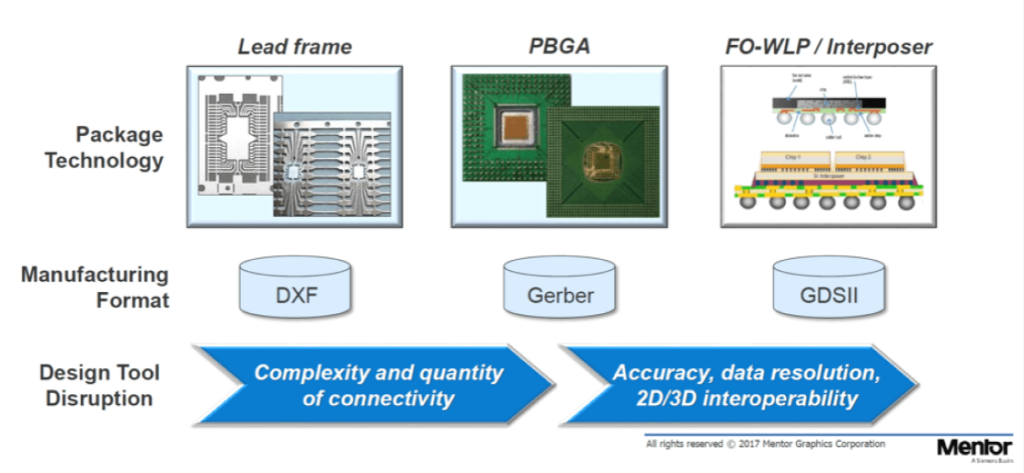
This comprehensive design flow also works for traditional packaging technologies, like flip-chip and wire-bonded system-in-package (SiP) designs. It provides design productivity, minimizes surprises, schedule slips and the risk of failure for interposer-based (2.5D) designs, chip-on-wafer-on-substrate (CoWoS) technology and fan-Out wafer-Level packages (FOWLP).
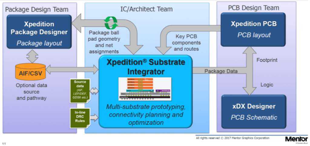
Figure 1 doesn’t show that this design flow manages different data formats and of course requires accurate inputs to produce valuable results. Figure 2 shows part of what Mentor’s developers had to deal with to facilitate the data flow between die, package, and board. Because it’s also very important to generate accurate and up-to-date design flow inputs and protect such proprietary data, Mentor offers methodologies to model, encrypt and express material characteristics and package capabilities in assembly design kits (ADKs). Based on many years of experience with developing process design kits (PDKs) with silicon foundries, they can also offer valuable advice for defining the ADK content and formats as well as generation and encryption of the data.
The end-to-end design flow Mentor announced this week, relies on many proven point tools, databases, and data formats. Figure 3 gives a closer look at the design tools and databases for the HDAP flow. It shows that Mentor managed to combine both Windows and Linux-based tools in this design flow. Figure 3 also shows (on the far left and far right) some of the inputs needed for this design flow.
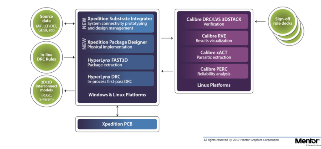
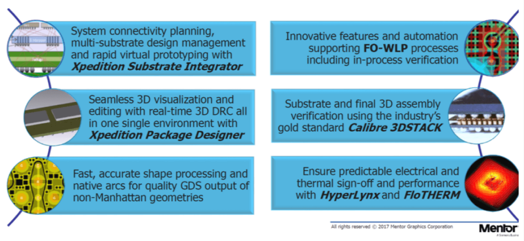
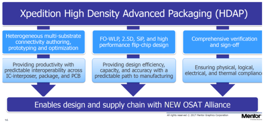
Figure 4 highlights some of the roles and benefits these Mentor tools offer.

Building a strong ecosystem for HDAP
As mentioned in the first paragraph, the success of an individual product, such as this HDAP flow, depends on its ecosystem. The key to success lies in supporting both the outsourced semiconductor assembly and test service providers (OSATS) and suppliers. That’s why Mentor also announced its OSAT Alliance program this week, modeled after the very successful Calibre foundry program and its PDK efforts. Mentor will work with OSATs to develop ADKs. As Figure 5 shows, these ADKs will increase productivity and predictability of all package related design steps at mutual customers. Amkor Technologies, Inc. is the first OSAT to participate in the Alliance program.
This blog can only convey a fraction of the information HDAP ecosystem partners and their mutual customers need, to assess the value of the end to end flow. Data sheets, white papers, in-depth expert presentations, training courses, even ways to get hands-on support found on Mentor’s website may be useful to show you the power of this design flow and how it can help differentiating your designs.
On a personal note:
Since 2008, when I started to promote multi-die ICs and advanced packaging technologies, I was hoping that, in addition to the many point tools EDA vendors started to offer, a user-friendly design flow would become available. Only a complete flow can really minimize risk, design time and cost of highly complex designs. Mentor’s end-to-end design solution, in conjunction with the OSAT Alliance program, will enable system and IC designers to meet today’s and future market demands for heterogeneous integration, higher performance per Watt, shorter time to market, lower development and unit cost and of course make IC designs more reliable.
In a few years, when you tell your self-driving car to get you from A to B, you want to be confident that you really will get there. This flow will significantly contribute to getting you from A to B, cost-effectively, comfortably and in one piece. ~ Herb
For detailed information about the capabilities of these tools, please go to Mentor’s website or contact your Mentor support person.


