
After spending three days in the company of the IMAPS community at the 15th annual IMAPS Device Packaging Conference (IMAPS DPC) March5-7,2019, in Fountain Hills, Arizona, I am once again reminded why I chose to focus 3D InCites on the advanced packaging segment of the semiconductor industry. The technology is fascinating and varied, the conversation is inspiring, and the people know how to have a good time.
This year was particularly significant for both 3D InCites and IMAPS DPC, as we celebrated our 10th and 15th anniversaries, respectively. Together, we represented 25 years of advanced packaging innovation. To commemorate the event, we hosted a barbecue during which we presented the 2019 3D InCites Awards and provided a photo booth for entertainment. The video below speaks for itself. I know, you WISH you had been there!
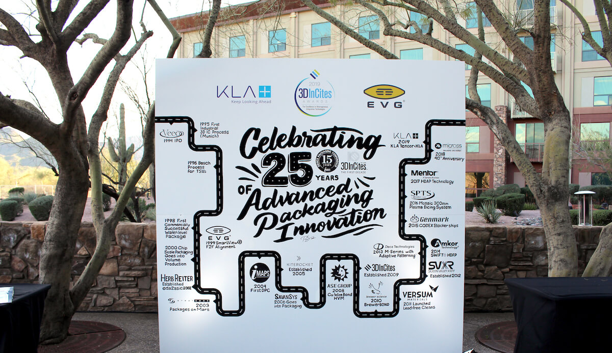
The theme of this year’s fundraiser mural, which allowed us to donate $3000 to the IMAPS Foundation, was, therefore, “Celebrating 25 Years of Advanced Packaging Innovation.” Participating companies sponsored milestones significant to them. Many of the sponsors were also exhibiting at IMAPS DPC, which gave me the opportunity to chat with them about the significance of the milestones. We’ll bring you this post in two parts: the first spans from 1994 to 2008.
1994: Veeco’s IPO
Counting back 25 years from 2019 brought us to 1994, the year Veeco went public. At the time, Veeco’s sales were approximately $30 million. A peek at Veeco’s history page revealed an interesting tidbit – the company started in 1945 as Vacuum Electronic Equipment Co, (pay attention, this could be a question on next year’s quiz) and specialized in leak detector equipment. It wasn’t until 1989 that Veeco shifted its focus to semiconductor equipment. The company has steadily acquired smaller equipment suppliers to build a process equipment-focused portfolio that spans semiconductor manufacturing from front-end processes through advanced wafer level packaging, and also plays in adjacent markets like LEDs and compound semiconductors.

1995-1998: Advanced Packaging Breakthroughs
Although no companies stepped forward to sponsor the years between 1994 and 1998, those years were still marked by some significant accomplishments. 1995 saw the first industrial 3D IC process proven by Fraunhofer EMFT and Siemens. In 1996, Bosch first published about using its deep reactive ion etch process for etching through silicon vias (TSVS). While 3D technologies were in early development stages, the first commercially successful wafer-level package hit the market in 1998.
1999: EV Group Introduces the SmartView Aligner™
With its early and ongoing activities in developing processes and tools for wafer level and 3D packaging, there were a number of milestones EV Group could have selected. 1999 was significant as it was the year the company entered advanced packaging space with the introduction of its SmartView® wafer-to-wafer alignment system, “which incorporates a revolutionary face-to-face alignment technology for wafer-level packaging technologies and 3D interconnects for hyper-integration.”
In acknowledgment of EV Group’s ongoing support for 3D InCites over the years, the company was featured in the cover story of our first print issue, commemorating the first decade of 3D InCites. Download the digital version here.
2000-2002 EDA Pays Attention to Packaging
Chip scale packages went into volume production in 2000, and with that, the radar of the EDA community went up. In 2002, Herb Reiter, well-known 3D InCites blogger, launched his consulting business, eda2asic, to help bridge the gap between electronic design automation (EDA) tool vendors and ASIC semiconductor companies. As advanced packaging became more significant, Herb shifted his focus from single-die ASIC solutions to integrating multiple dies into an IC package to bridge the many gaps between partners of this complex ecosystem.

2003: StratEdge Packages on Mars
Recent news reports revealed that after 15 years of faithful transmission, Mars Rover, Opportunity, officially went dark, having sent its final message in June 2019. Because Opportunity was only expected to survive three months, making it to 15 years was nothing short of remarkable. This news was significant to me, because in my early days at Advanced Packaging Magazine, I visited StratEdge’s headquarters in Santee, CA, and learned that their packages were on the Mars Rover. I reminisced about that visit with StratEdge’s Tim Going and Casey Krawiec, and the sad news about Opportunity. Going pointed out that the packages were so reliable, they weren’t the reason the Rover finally failed. It’s battery just finally died.

While StratEdge is still focused on packaging high-performance, high-frequency compound semiconductors for military and aerospace, they’ve also entered the 5G space, focusing on assembly and packaging for gallium nitride (GaN) devices that require a different approach to assembly and packaging the more traditional gallium arsenide (GaAs) power packages, according to Krawiec. Specifically, they’ve developed high-frequency, high-speed, thermally efficient, leaded laminate copper-moly-copper (CMC) base packages for GaN devices. “When GaN is integrated, it works better than GaAs at higher frequencies.” Explained Krawiec. “5G will be a great space for us.”
2004-2006: WLP Gets Real
As wafer level packaging technologies took hold, it opened up a new focus for iMAPs. In addition to the annual international technology symposium held each fall, the organizing committee kicked off a second international event, the International Device Packaging Conference (DPC), held each year in March since 2004 in Fountain Hills, AZ. The 2019 conference welcomed nearly 600 attendees from 15 countries, four technology tracks included:
• 3D applications and technologies
• Flip chip, wafer level packaging, and fan-out
• Engineered microsystems/devices (including MEMS, sensors & 3D printing)
• Automotive packaging
The 2005 milestone acknowledges the year Kiterocket, a full-service PR and marketing agency, was established. With deep roots in the semiconductor and advanced packaging industries, the agency represents numerous companies across the semiconductor supply chain.
Savansys Solutions, LLC, is in the business of electronics supply chain cost modeling using a combination of consulting and unique, proprietary software. 2006 was the year the company first put its activity-based cost modeling methodology to use in the advanced packaging market. Since then, the team has provided clients across the supply chain with useful cost analyses of every type of packaging approach, from wire bond to flip chip and fan-out to 3D integration technologies.
2008: ASE Goes Big with Cu Wire Bonding
2008 was significant for Advanced Semiconductor Engineering, Inc. (ASE) because it’s the year the outsourced semiconductor assembly and test (OSAT) giant took copper wire bonding into high volume production.
The company most recent significant milestone took place in April of 2018 when it completed its joint share agreement with Siliconware Precision Industries Ltd. (SPIL). The merger of the two companies under the new name, ASE Technology Holdings Ltd. make it the largest OSAT in the world.
So what happened next? Read on for more.


