
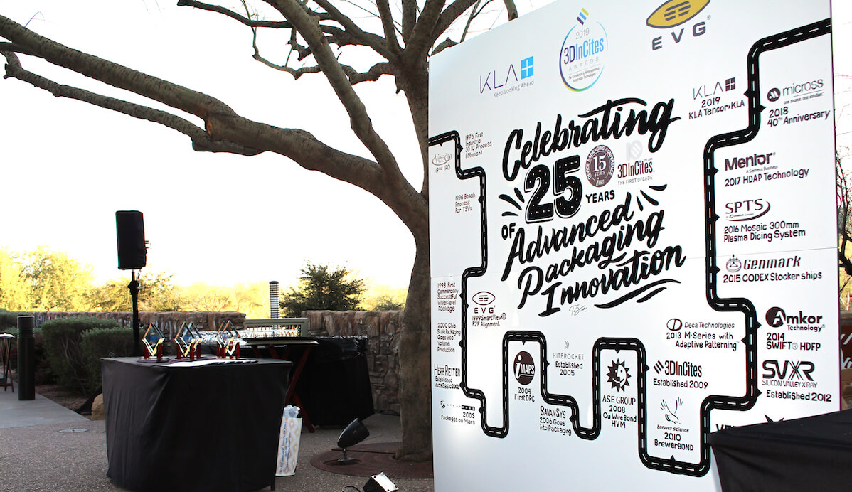
Picking up where we left off , Part two of this series celebrating advanced packaging innovation takes us from 2009-2019, beginning with the establishment of 3D InCites in 2009. The first conference I covered was the IMAPS Device Packaging Conference in 2009. We officially launched the first website in time for SEMICON West 2009. Remember the logo? Things could only improve from here.
In 2012, now in partnership with Martijn Pierik and Dave Richardson, Impress Labs, we re-branded the site with a new logo and design as it appears today. There’s more to the story here.
2010: Brewer Science introduces BrewerBond™
For years, the temporary bond/debond step for thin wafer handling in 3D integration and fan-out packaging processes was plagued with challenges. In 2010, Brewer Science introduced its breakthrough technology, dubbed BrewerBond, to address challenges mostly associated with the debonding step, such as delamination. This product family reportedly improves throughput, simplifies cleaning, and shortens the processing time. The company has continued to evolve this product line to adapt to various applications needs, providing a solution for fan-out, 3D ICs, MEMS, power, and compound semiconductor applications.
2011: Versum Launches Lead-free Cleans

To comply with the OSATS transition to lead-free solder bumping in 2010, Versum Materials brought its lead-free cleans products into high volume manufacturing in 2011. Prior to that cleans involved eutectic and high-lead solders and required a different formulation to be compatible with lead-free solders, explained Diane Scheele, business manager, Versum. This work puts the company in a good position now in 2019, as automotive is shifting to lead-free materials.
As we’ve discussed before in articles about the importance of cleans, it’s really about device reliability and surface preparation, and the importance of materials compatibility for the next step in the process. At IMAPS DPC, Versum co-presented a poster with SPTS Technologies on removing fluorinated residues from the singulated die on tape after plasma dicing. The first adopters of plasma dicing are small die power semiconductors, which are a growth market, as we learned during the Global Business Council.
2012: SVXR Established
 After spending 12 years developing a new X-ray inspection system specifically for inspecting advanced packages that is 100X faster than existing imaging tech, David Adler, former chief technologist at KLA, co-founded Silicon Valley X-ray (SVXR) in 2012, along with Scott Jeweler, a packaging industry veteran.
According to Adler, the company is on a mission to offer an alternative to automated optical inspection (AOI) for advanced packaging inspection, particularly solder ball joints between package layers that can’t be seen with AOI. Adler explained that existing systems are based on X-ray microscopes used in the lab that operate at 1-10 units per hour. While the images are high resolution, the process is too slow for inline inspection. Two things are needed to go from lab to inline: images must be taken quickly, and data must be processed in real time.
“To design an X-ray system with a throughput of 1000 units/per hour we had to throw out everything that was available about X-ray technology and start from scratch,” said Adler. “We started with developing a new source and detector, and developed algorithms that can manage extremely high data throughput of 1000 connections per second and can measure the quality if the solder and the connection.”
Imaging speed and machine learning (ML) for defect detection with high enough reliability for an inline semiconductor application are two technology innovations that made SVXR’s 100X improvement possible. “Two years ago, we couldn’t do what we do now, because ML wasn’t what it is today,” noted Adler.
2013: Deca Technologies introduces M-Series™
M-Series with Adaptive Patterning™ is Deca Technologies’ fan-out packaging technology that is rapidly changing the fan-out landscape. While the technology was slow to be recognized industry-wide. It is now being rapidly adopted for mobile chipsets because its face-up die placement and fully molded structure is improving board-level reliability.
2014: Amkor Technology, Inc. Introduces SWIFT™ HDFO

While Amkor selected 2014 for its milestone, recognizing the introduction of its high-density fan-out offering, SWIFT, that’s not what I talked about with Amkor’s Mark Mangrum. Rather, we talked about how the company not only invests in developing new leading-edge technology (such as SWIFT HDFO), but also continues to invest in existing package types that are alive and well, and being used more than ever, such as quad flat no-lead (QFNs) and Microleadframes (MLF).
Why? “They (automotive manufacturers) hate new,” says Mangrum. “Devices need to be well proven. Automotive is not a testing ground for new technology.”
So instead of new, Amkor innovates to build a better mousetrap. QFNs and MLFs in particular, are growth centers for semiconductor packaging within automotive applications. Once designed into an automotive application, the devices need to last 7-10 years.
Mangrum presented two papers at IMAPS DPC. One on a wettable flank technology that enables solder joint inspection. The other on edge protection for QFN packages. The former describes forming a solder joint so that a filet (or flank) forms, thereby validating that the solder joint was actually formed under the package. This enables automotive and PCB assemblers to inspect joints using a new type of AOI equipment that can determine the quality of the filet. This eliminates the need for manual inspection and X-ray inspection, reducing cost.
Edge protection is an innovation developed for punch singulation of QFN packages, to protect the edges of the devices during handling and test. It improves the robustness of the package by 2X and stops the cracking.
2015: Genmark Automation Ships First CODEX Stocker

Also introduced to the market in 2015, Genmark Automation’ CODEX stocker is a stand-alone automated handling system that integrates metrology, stocking and sorting into one system apart from processing tools. That same year, I interviewed Carl McMahon, EVP sales and marketing worldwide for Genmark, about how this tool suits the varied handling and cleaning requirements that come with TSV fabrication, as well as the lack of standards set for interposer integration and 3D ICs. You can find that blog here.

In four short years since its introduction, CODEX is taking the industry by a storm, shipping five Codex stocker and storage systems in the advanced packaging market. He expects to hit double digits with the number of systems shipped by 2020. That notoriety won Genmark the 2019 3D InCites Equipment Supplier of the Year award.
2016: SPTS Introduces MOSAIC Plasma Dicing System

Best known for its deep reactive ion etch (DRIE) process tools for forming through silicon vias (TSVs), SPTS got into the dicing business with DRIE in 2016 with the introduction of its MOSAIC Plasma Dicing System.
In comparison with saw dicing, plasma dicing doesn’t damage the wafer or the trench sidewall, resulting in greater die strengths, improved device reliability and increased device lifetime. Because dicing streets can be <5µm, it’s possible to fit 100% more die on a wafer. The shape of the die isn’t limited to square – with plasma dicing the die can be any shape that accommodates the wafer best.
While it’s not the only plasma dicing game in town, according to Jeff Dumas, central regional sales manager, SPTS, its dual source RF gives it the fastest etch rate on the market at 20µm per minute. The company also lays claim to the largest plasma dicing install base, with tools for both dice before grind (DBG) and dice after grind (DAG). Endpoint protection allows for dicing with plasma on tape. The process is device agnostic and can be used for standard Si die, compound semiconductors, and GaAs, as well as FOWLP.
Dumas noted that plasma dicing works best when die are designed with no metal in the streets because DRIE won’t clear metal in the lanes. If there is metal in the street, you must pause DRIE, laser ablate them metal and then finish DRIE. Therefore, it’s important to consider the plasma dicing process in the initial die design.
2017: Mentor: High-Density Advanced Packaging

According to Kevin Rinebold, Mentor, 2017 was a significant year for the promotion of HDAP, terminology developed by Mentor as a way to differentiate the focus area for its design tools, Xpedition and Calibre. HDAP is defined as disruptive packaging technology that forced the change in tools and methodology, causing companies to update their design tools in three main areas: planning and prototyping; assembly verification; and physical implementation.
“Heterogeneous integration was a disruptive influence on design methodology,” explained Rinebold. “Assembly verification is one of the biggest areas of disruption as it can involve different die with different patterns from different companies.”
2018: Micross Celebrates its 40th Anniversary
 Choosing a milestone was easy for Micross, as 2018 was available and it’s the year the company celebrated its 40th anniversary. I caught up with Alan Huffman, who updated me on the activities of the advanced interconnect technology (AIT) division of Micross, where all the 3D stuff happens. Huffman said the company has been busy with various government development programs in aerospace and defense, as wells as collaborative projects, such as with the DARPA CHIPS program developing fine-pitch interconnects, TSVs and silicon interposers.
At IMAPS DPC, however, he was promoting not just the AIT division, but the entire company as a service provider. Micross services offering includes die sales, wafer-level bumping, 2.5D, and 3D assembly and test. “We do it all, but we’re not competing with the OSATS,” explained Huffman. Nor does the company play in the consumer electronics space. Rather, the company’s sweet spot is supporting low-volume, high-reliability devices that need on-shore providers who can meet the requirements for quality and consistency of supply.
2019: KLA Tencor Rebrands as KLA

January marked a new beginning for KLA Tencor, a provider of advanced process control solutions. Not only did they change the name of the company to KLA Corporation, but it also rebranded and adopted the tagline; Keep Looking Ahead™, to indicate KLA’s optimistic view of technology’s impact on the world. In the vision statement posted on the freshly designed website reads:
Why We Believe in a Brighter Future
It’s our belief at KLA that innovators are true optimists. We take on complex technical challenges that often take years to solve. We work on the edges of deep science, exploring electron and photon optics, sensors, machine learning, and data analytics. We help create the ideas and devices that transform the future.
That’s a Wrap

Both as KLA-Tencor and KLA, the company has been a platinum sponsor of the 3D InCites Awards for four consecutive years and participated in the festivities. Last year, Team KLA, led by Steve Hiebert, won the quiz. This year, despite a heroic effort by this year’s team captain, Go Nagatani, Team EVG, lead by Garrett Oakes, took home the prize. Literally. They got to take home the mural.


