
Because IMAPS is a society, there is a strong community aspect to its events. It was good to see that captured at this year’s symposium. I really enjoyed attending the live versions of the Society Awards presentation and the Diversity and Inclusion Roundtable. I also popped into the Student-Industry Roundtable discussion.
I was very pleased to see a number of the 3D InCites Community received accolades.
- Leadership Award – Rozalia Beica, AT&S, and 3D InCites Technical Advisory Board
- President’s Award – Curtis Zwenger, Amkor Technologies
- Corporate Recognition Award – ASE
Congratulations to all! The complete list of winners can be found here.
I was really impressed with the conversations taking place during the Diversity and Inclusion Roundtable. The integrated Zoom platform made it possible to have a real conversation. 50 attendees comprising both women and men, as well as a number of student members. People shared programs/initiatives their companies are running and asking compelling questions. Now that everyone has recognized that the advantages of DI, efforts are well underway to adapt to hiring practices, but it’s proving to be more challenging than expected. It’s clear that the change we want to see will not happen overnight. It’s a slow progression that requires many initiatives. We really need to reach out to students as young as middle school age to teach them about this exciting industry, and the opportunities that await them.
My IMAPS Virtual Event Score Card
I have to call it as I see it. As a virtual event, the 2020 IMAPS International Symposium’s strength is definitely in its program content. The keynote speakers presented compelling talks. Likewise, Jan Vardaman’s panel discussion was probably one of the most interesting I’ve ever attended – not only because it was a compelling topic with topnotch panelists – but because of the Zoom platform that created more of a round-table discussion format.
The virtual exhibit portion of the event was fairly disappointing, especially, if like me, you carved out part of your day to actually engage and network with the booth attendees. I visited every single exhibit, hoping to connect with some live bodies (either in a chat of a video conference), and came up rather short, partly due to what appeared to be a low-budget platform, and partly due to the exhibitors who didn’t make the most of the space they had to work with, except for a few.
A Tech Round-up of One
I generally write a tech round-up based on face-to-face conversations I have with exhibitors. Unfortunately, only three exhibitors, Canon, Materion, and ASE, had enabled video chat using Zoom or Microsoft Teams. Nobody “answered” my call at Materion, so I moved on to Canon. Doug Shelton was delighted to chat – “You’re the first person I’ve talked to all day!”. He brought his colleague, Takaaki Tsunoda based in Japan, into the conversation. This was cool, as it could only happen with a virtual event. I had never met either of them before, so it was great to learn a bit about what Canon does in the heterogeneous integration space.
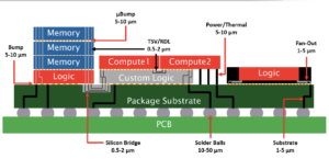
After briefly explaining Canon’s 50 years in the lithography business, Shelton explained the company’s decision not to pursue EUV and pivoted instead to focus on nano-imprint lithography using a quartz stamp that is etched, rather than an optical approach. He says these tools will be able to support the 5nm process. Canon’s big news of the show was the introduction of its panel stepper and the introduction of the fine panel aligner. The tool supports 510-515 mm panel sizes, processes 40 panels per hour, and has an image field size of 55mm x 55mm, allowing it to image a large device pattern without stitching. While the system can handle glass panels, it’s designed for copper-clad (CCL) substrates used in fan-out panel-level packaging. Shelton said it can handle RDL patterning down to 1/1 line/space and can create etch masks for TSVs.

Tsunoda-san supports Canon’s Anelva Group, focusing on tools for physical vapor deposition, etch, bonding, and X-ray. He walked me through the sputtering and hybrid bonding capabilities to create compound semiconductor wafers. Of interest to our readers is the company’s novel X-ray source developed to inspect fine features. This component provides high resolution and very high power to inspect many devices at one time and is suited to wire-bond inspection, as well as voids in BGAs.
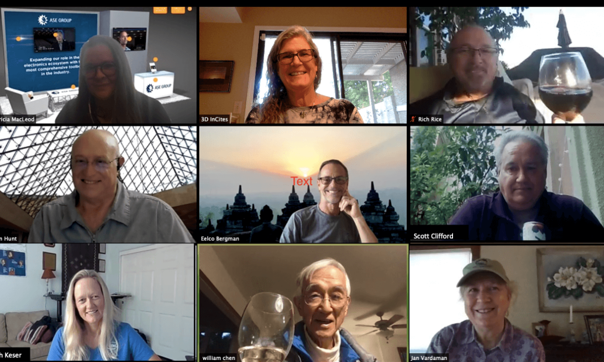
IMAPS Happy Hour at ASE
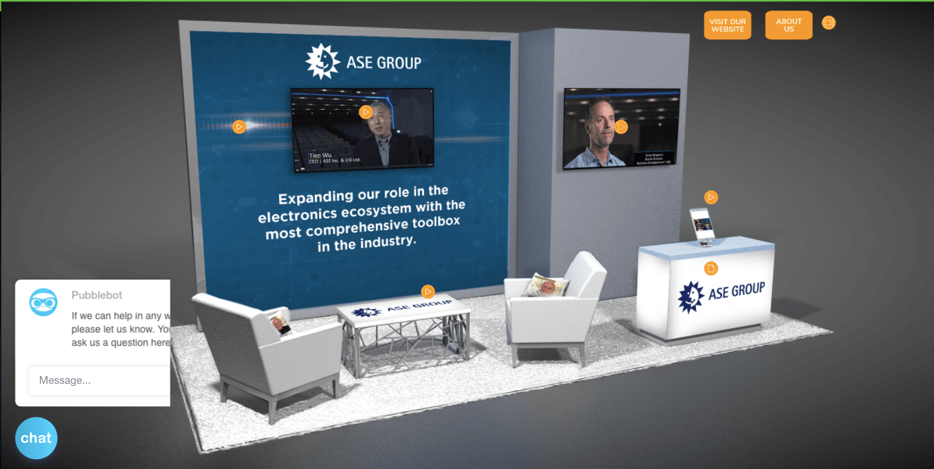
After a busy few days, it was nice to kick back for a Zoom Happy Hour with the team at ASE, and Jan Vardaman. We re-hashed the best parts of the conference and shared some thoughts on how to improve the virtual experience. ASE’s Patricia Mcleod did a great job making the most of their virtual exhibit, developing video content for the booth, including a welcome video, John Hunt talking fan-out, a message from CEO Tien Wu, Mark Gerber on 5G, and what’s on the minds of all the technologists. It’s worth the free registration to check them out here.
IMAPS Symposium content is still available for one more week and it’s not too late to registers. If you go, check out our community members presented technical papers in the heterogeneous integration and 3D tracks including:
- Bill Chen, ASE, HIR Overview and HIR Roadmap Highlights
- Aric Shorey, Mosiac Microsystems, Thin Glass Handling Solutions for Microelectronics Packaging
- Sudhakar Raman, Brennan Peterson, SVXR, Inc., Optimizing Package Yield and Reliability with X-ray Inspection


