
These days, the first thing that comes to mind when someone mentions fan-out (FO) technology is Apple’s A10 processor built on TSMCs integrated fan-out (InFO) technology. It’s the superstar application that put FO on the map and into high volume manufacturing.
However, equally important to remember are the numerous low-density FO workhorses supporting other mobile applications, as well as markets beyond mobile. They come in a variety of acronyms from all the leading outsourced semiconductor assembly and test service providers (eWLB, SWIFT, eSiFO, ECP, RCP, TPI-FO, etc). One technology stands out for, among other things, not having an acronym-based name: Deca Technologies’ M-Series.
In the continuation of our 3D InCites Award Winners series, I spoke with Chris Scanlan, Sr. VP of product management and engineering, Deca Technologies, to learn more about how the low-density area of the fan-out landscape is evolving, and how it will impact the future of heterogeneous integration, and the role M-Series plays in all of this.
LDFO applications
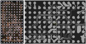
Initial applications for low-density FO (LDFO) packages are in mobile chipsets, supporting devices other than the application processor and modem, explained Scanlan. These include power management ICs, CODECs, and RF ICs. Beyond mobile, LDFO is already being used in automotive electronics for advanced drivers assist systems (ADAS) transceiver chips because it provides improved RF performance. Additionally, noted Scanlan, the FO structure offers additional benefits in terms of reliability and performance enhancements, so will likely be a key player in automotive going forward (Figure 1).
Challenges facing LDFO
Low-density applications have now reached high volume manufacturing. While there are multiple architectural FO choices, they aren’t in HVM, nor are they multi-sourced. Scanlan noted that ultimately, as with the adoption of flip chip packages, the market will decide what technology is best. What they need are multiple-supplier sources. For example, eWLB – which stands for embedded wafer level ball grid array (eWLB) is well established, has been qualified since 2008, and has been licensed to multiple suppliers.
Indeed, Scanlan identified one of the key barriers to broad adoption for new FO technologies is how to enable dual or multi-sourcing. “At Deca, we’ve addressed that with our relationship with ASE,” he said. “They invested in Deca, and we’ve co-developed and licensed our technology with them.” The technology he’s referring to is Deca’s M-Series fan-out platform.
A Different Approach
Deca Technologies’ M-Series is a fan-out platform that is built a little differently than the others and is beginning to make a name for itself. Scanlan explained that in comparison with face-down architectures like eWLB, in which the chip is literally placed face down on a temporary carrier for molding, in M-Series, chips are placed with the active layer face up and then molded over the top in a continuous layer to fully encapsulate and encase the chips. Cu studs are plated on the Si wafer to provide interconnect between the die and fan-out RDL (Figure 2). This fully molded structure provides better mechanical protection for the active side of the device and provides an additional buffer layer between the die and BGA array. “This allows us to improve board level reliability,” said Scanlan “In fact, for designs that call for placing solder balls in the die shadow region, we can put them over the die edge without a significant reduction in board level reliability.” This is why M-Series is being adopted for mobile chipsets, where traditional wafer-level chip-scale packages above 5mm die size are no longer adequately reliable.
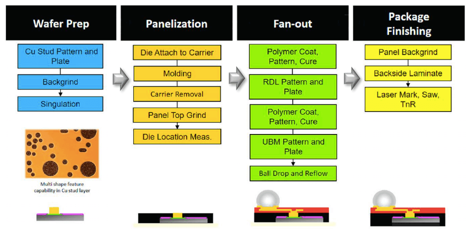
The main structural difference between eWLB and M-Series is the proximity of the fan-out redistribution layer (RDL) to the surface of the chip. In the case of M-Series, a layer of mold compound encapsulates the active side of the chip and the mold is planarized to reveal the copper (Cu) studs, then the RDL is formed on top of the Cu studs which are coplanar with the mold compound. “This also ensures chip-package interaction reliability while protecting the low-k dielectric layers on the die,” explained Scanlan. The Cu stud layer can also be used to enhance thermal performance, and as it doesn’t use a solder cap, it can accommodate bumps of various sizes and shapes within the same die. The increased gap between the die and RDL also eliminates the risk of shorting due to metal burrs created in the wafer saw process.
Another key differentiator is Deca’s proprietary Adaptive Patterning, which solves the die shift issue on-the-fly by using optics and measurement to determine the position and rotation of each die, then creates an optimized design for each unit for RDL patterning. According to Scanlan, this improves assembly yield and allows for a lower cost die placement process.
Deca competitors say the technology is interesting, but it’s still not proven in HVM. To that, Scanlan says while M-Series hasn’t been ramped into HVM yet, it’s been qualified for HVM applications, and we can expect to see examples of M-Series in consumer products later this year.
ASE’s role
ASE is already offering at least seven varieties of FO technologies, of which M-Series is one. These options will all co-exist as they are optimized for different applications. What are the advantages of this partnership?

“Our relationship with ASE enables dual sourcing of M-series technology, which enables customers with large volumes because they can place orders with both companies,” said Scanlan. “Additionally, our licensing and transfer agreement allows us to collaborate to ensure the manufacturing structure is identical, which is critical to the supply chain.”
A word about panel level packaging
Deca’s original claim to fame is its solar-inspired flow line wafer fabrication process used for its fan-in technology. The process uses some large-scale equipment similar to that used in panel level packaging. Panel-level packaging is very much talked about for fan-out technologies, but skeptics say there aren’t enough volumes needed to justify the investment.
Scanlan acknowledged that large panel format is not viable for low-volume applications, however as FO grows in the mobile space, which demands billions of units, it makes sense to adopt it to reduce cost. To this end, Deca and ASE are collaborating to extend the technology to large-panel format, as well as extending it to address other areas of the market (Figure 3). The belief is that roadmap to large panel format provides a roadmap to cost reduction in the future.
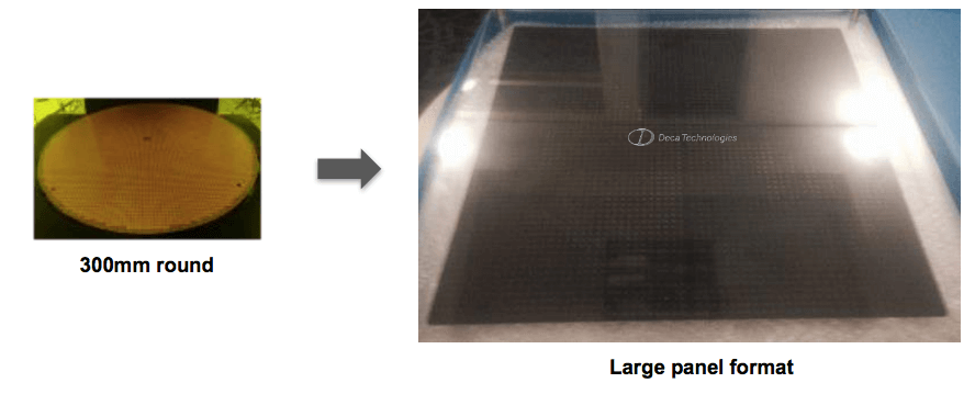
Their approach is to create a large panel manufacturing process that produces parts that are structurally identical to those produced in the 300mm round format so that either line can be used for a given product. That way a design can start on 300mm round and transition to the large-panel format as volumes increase.
Looking forward
“First and foremost, M-series is a platform because we can address multiple applications spaces with the core technology,” said Scanlan. “We’re already doing multi-die M-series. Adaptive Patterning is key to achieving high yields on higher density designs, particularly with multi-chip and larger die sizes.”

While it is being implemented first in LDFO applications, there are bigger plans in the works, such as FO system-in-package (FO SIP) using a large panel and implementing surface mount technology. Scanlan presented on that topic at last year’s 3D ASIP conference. The portfolio is expanding to high-density approaches, with milestones like <2µm l/s line density multiple RDL layers, and 3D structures marked on the roadmap. M-Series also has potential as a motherboard replacement to create and end-system, and in lieu of interposers for HD applications.


Comments are closed.