

Two schools of thought clearly emerged at last week’s European 3D TSV Summit, which took place on January 20 and 21, 2014 at Minatec campus in Grenoble France. One I addressed in yesterday’s post – about realizing system-level benefits – including cost – by integrating 2.5D and 3D IC technologies. The other big question mark, as we all know, is how to reduce the cost-of-ownership of these technologies so that they can be implemented in consumer mobile applications.
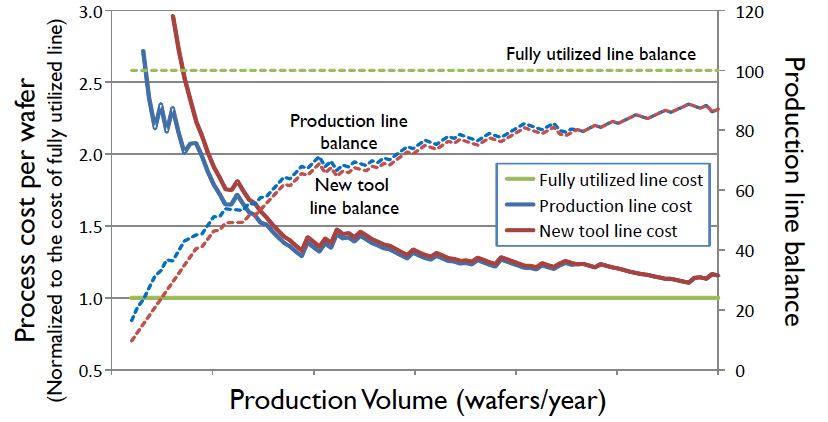
Eric Beyne, director of 3D System Integration Program at imec, has been working to improve cost-of-ownership and presented a comprehensive cost analysis along with process optimizing recommendations for both 3D and 2.5D interposers. He says we have to look beyond just the cost of TSV itself and include all cost aspects of 3D technology as well as other external factors, like CAPEX and units per hour (UPH), fab volume, depreciation, infrastructure, etc. He offered a comparison of volume and process line balance dependence to explain how the costs can be affected based on line utilization (Figure 1). Essentially, low volume production leads to unbalanced production lines and therefore increased process costs.
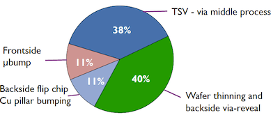
Beyne then provided a relative wafer level cost breakdown of a 3D IC process flow based on a fully utilized and balanced line (Figure 2). What’s interesting is that although it appears that the TSV middle process and the wafer thinning and backside process steps are the most costly, when broken down further, we see the step by step analysis of what the cost culprits are (Figure 3.)
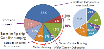
Beyne’s analyses lead to the following key takeaways for TSV cost of ownership reduction. First all, cost of CMP is a dominant factor, and whatever can be done to reduce the cost here will be significant. He suggests:
- Reducing Cu overburden after TSV fill
- Improving liner conformality across the wafer surface and TSV sidewall.
- Reduce barrier and seed thickness
Beyond CMP, Beyne says cost reductions can be achieved by increasing the via fill speed of electrochemical deposition processes (ECD) and reducing fill volume of TSVs by having smaller diameters and shallow depth. Additionally, finding a way to increase etch speed without reducing within-wafer (WiW) uniformity or degrading sidewall quality would also help.
Beyne’s recommendations for wafer thinning and backside process cost of ownership reduction were to reduce the complexity of the temporary carrier process, and minimize post-thinning CMP (he also discussed this last year at the 2013 European TSV Summit). He also advocated a via reveal process that incorporates endpoint detection – such as those offered by SPTS (dry etch) and SSEC (wet etch). He also offered a way to avoid the redistribution layer (RDL) and bumping steps altogether by using the Cu revealed TSV as the backside bump.
In his presentation on improved etch rates for via reveal processes, David Butler, SPTS, provided some results on work done with imec targeting 1µm high via tips. He reported achieving the 1µm high tips with a 0.1μm range of uniformity across batch at the wafer center and 0.6μm at the edge.

I talked to Beyne to get more details on using the revealed TSV as the backside bump. He explained that this is done by controlling the thickness of the die as you thin, and having good control of the TSV depth thanks to endpoint detection. The backside wafer can be recessed using wet or dry etch without grinding or removing the TSV. The remaining TSV “self bump” is wrapped in oxide and not damaged. The oxide is removed by backside passivation, and RDL and backside bumping processes can be eliminated. All the lithography steps required for Cu pillar on the backside are eliminated, thereby reducing cost of ownership. “The cheapest things are the things you don’t do,” quipped Beyne. The TSV self bump is a very good approach for fine-pitch TSVs beyond 20µm pitch, noted Beyne. This leads to the question of testability. Beyne said that its tested on the front side, and inspection becomes more important. Memory stacks is the target application for this approach.
On the 2.5D front, Beyne also examined interposer-based stacking from a cost-of-ownership perspective. He noted that while it is similar to 3D stacking, it also includes multiple interconnect layers. He said it is highly sensitive to die and interposer yield, so test is critical to avoid high cost due to compound yield reduction.
While larger substrates allow for more interposers per wafer and better utilization, there is new equipment and infrastructure to consider, and more volume to achieve low cost targets. With regards to Si or glass as a substrate to lower cost, Beyne explained that changing from Si to glass “is not going to hit the magic bullet, because all the other elements are still there.” Cu/oxide damascene Si interposer technology offers the highest interconnect density. But ultimately, Beyne says direct 3D stacking offers the highest interconnect density at the lowest cost. ~ F.v.T.


Francoise
Thanks as always for your summary. On the 2 key take away items of benefits of 3D I wanted to share some thoughts from my side.
1. Benefits of 3D: As noted, you have outlined this well in your previous post, and overall I believe the industry as a whole shares a similar perception.
2. CoO and adoption in a consumer application space. I wanted to highlight that has already been established via the Sony BSI CIS w/ interconnect. Ziptronix ZiBond(r) and DBI(r) Technologies (Sony has licensed ZiBond(r)) enable 3D & 3D w/ Interconnect utilizing industry standard tools and processes that are readily available and in use in most fabs today. DBI(r) can effectively eliminate the cost and challenges associated with TSV’s as a result of the DBI(r) process and when compared to alternative interconnect technologies can be as much as 4x less costly an option, with greater scalability.
HI Rick –
Yes – I hear references to DBI more and more frequently in my discussions, in particular in conjunction with BSI CIS. Thanks for your comment.
What are the yield assumptions for Fig 3, especially bond / debond ? Beyond that what about the stress effects of Cu – filled vias ? At IMEC have n’t they heard about Tezzaron yet ? Seems that Govt. funding for R&D in the socialized European environment allows one the luxury of not being result oriented. Why even waste bandwidth / technical credibility covering them ?
On the other hand its great to see smart result oriented Winners like Ziptronix & Tezzaron now working together.
Dev,
Eric did not mention yield assumptions, He presented his cost exploration work being done at imec as a relative comparison, not absolute numbers, because as he stated, there are many factors that affect overall cost. The point of this cost modeling is to identify key areas of the process flow that would benefit from process optimization to reduce cost of ownership. How is that not result-oriented? He did not address the stress effects of Cu filled vias because that was not the focus of the presentation. I don’t consider any of this coverage a waste of bandwidth or technical credibility. 3D InCites is meant to be a forum for discussion and my job is to report on what is discussed at the conferences I attend to keep my readers informed.
I also disagree strongly with your jab at EU funded research. This funding encourages collaboration between R&D centers and EU industrial partners that leads to real products in the market, like those being manufactured at ST Micro, ams, Infineon and Siemens, to name only a few. I believe there is much to learn from the EU approach investment in technology innovations.
Francoise,
Thank you, and yes the value proposition for BSI CIS with Ziptronix technologies have been received well, and as noted (With Thanks) by Dr. Gupta in the Memory space as example with Tezzaron. Another exciting area is in the SoC space and the cost savings that can potentially be realized when considering 2D vs. 3D. We have done cost modeling on this, and if you or anyone are interested, please contact Ziptronix. We will soon be launching a support tool on the Ziptronix web site. Stay tuned.