
Stacking transistors on top of each other sequentially in the same front-end process flow is a concept that has been imagined to provide the semiconductor community with an alternative to the traditional scaling paradigm challenged by technical and cost roadblocks. LETI Advanced CMOS Laboratory introduced CoolCube™, a low-temperature process flow that provides a true path to 3DVLSI.
Limits of 2D-Scaling
Since the commercialization of the first microprocessor by Intel in 1971, the miniaturization of transistors has been the main engine of the semiconductor market’s growth. This growth followed the empirical Moore’s Law (named after Gordon Moore first CEO and creator of Intel); namely the doubling of transistor density every two years. This 2D-planar integration has consistently enabled semiconductor players to provide new product ICs with improved operating speed and performances at lower costs.
However, with the extreme size reduction of today’s most advanced generations, parasitic phenomena appear such as: short channel effects, increased gate leakage variability, increased static and dynamic consumption. To address these issues, new materials have been introduced (for gate stack, channel and the contact access). The industry resorted to strain management and architectural changes were proposed (SOI transistors, double gate, multi-channel transistors, FinFets, …).
On the other hand, the number of transistors on chips is increasing, as well as the length of metal wires connecting them. Delays in these interconnections limit the performance of integrated circuits. They reduce the performance improvements at the transistor level. To address this challenge, aluminum was replaced by copper; and less resistive, dielectric insulators were made porous to lower the capacitance coupling between metal lines. Despite these technological efforts, delay in interconnects still limits the performance of integrated circuits (Figure 1).
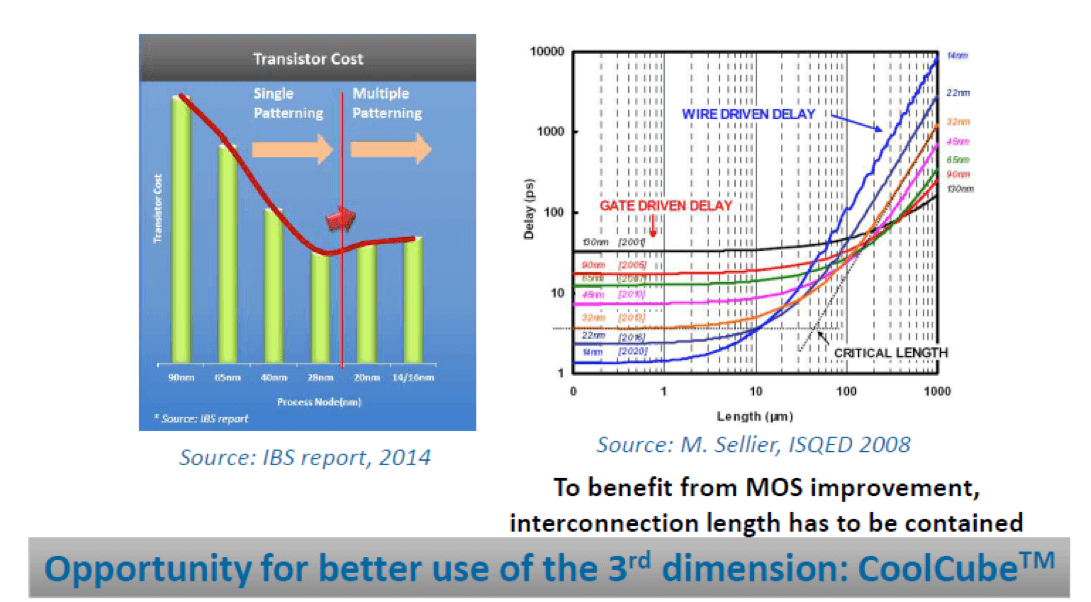
All these difficulties can no longer be tackled through innovation based on Moore’s Law applied to a unitary device: performance has certainly increased but investment and production costs get more challenging for new devices compared to previous generations. These limits have increased the interest of the semiconductor industry in 3D integration concepts: one can not only use the reduction in size of the devices but also optimize the IC interconnections by stacking devices on top of each other. This 3D way of thinking provides many advantages over a planar integration, including:
- The possibility of increasing the density of transistors per unit area without necessarily reducing their size (limiting noise effects due to the miniaturization and related costs).
- The opportunity to improve the performance of integrated circuits via a time gain in the interconnections through the replacement of long horizontal interconnects by shorter vertical interconnections, also by the independent optimization of devices made on separate levels.
- The simplification of heterogeneous technology co-integration.
There are two main technological routes to achieve 3D Integration:
- Parallel integration, in which two layers are first manufactured in parallel and bonded together to produce the three-dimensional stack.
- Sequential integration, in which the different layers of transistors are manufactured sequentially one after the other on the same substrate.
The main difference between both integration schemes is the density of interconnections between the layers (Figure 2).
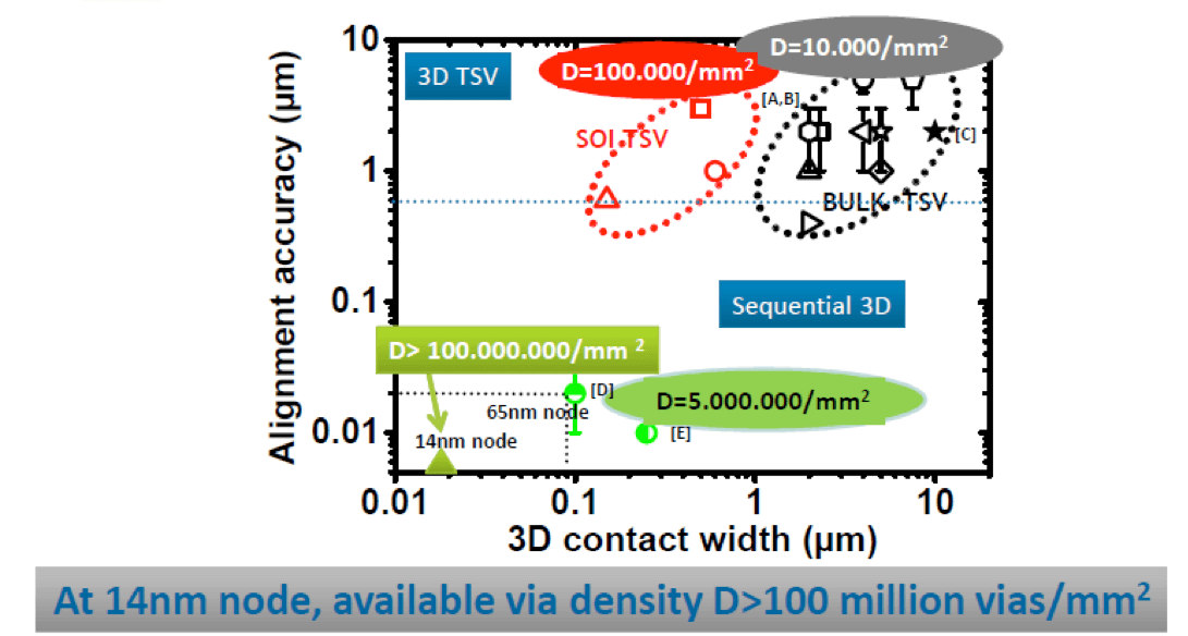
In the parallel integration scheme, alignment accuracy between the two substrates that are manufactured separately and then assembled is limited by mechanical alignment precision. In addition, the thickness of each process wafer is such that the via connecting the bottom plate is deeper than a conventional plug, consequently, it prevents the diameter of this via from being in the tens of nm, thus limiting the number of holes per unit area. Indeed, the drilling processes of these vias are physically and chemically limited to a depth / diameter ratio.
In the case of sequential integration, once the bottom wafer has been processed, the upper device is manufactured by integrating the connection vias through very thin layers. These 3D vias can be achieved using a photolithography process conventionally used in the semiconductor industry. Photolithography achieves precision and order of pattern density equal to transistor’s dimensions themselves, alignment precision only depends on the lithographic alignment capability of the stepper. In the case of the sequential integration, connection density is up to 1000 times greater than parallel integration.
LETI Offering CoolCube™
LETI is recognized for its expertise in key fields of knowledge needed to validate and implement the sequential 3D concept:
- A strong background in FDSOI technology and its related use of silicon-on-insulator (SOI) wafers
- A long history of process developments for molecular bonding of various substrates and materials
- A thorough experience of 3D stacking techniques including design tools developments, architecture exploration and test vehicle or full circuit implementations
- A competence center in complex SoC design and in system architecture development.
LETI’s Advanced CMOS device laboratory activities are exploring many paths for future generations of semiconductor devices. Among multiple research domains, sequential 3D integration is our main thrust for investigating alternative routes to scaling, with a program launched in the mid 2000’s.To achieve expected performance with a right time to market, the CoolCube concept must be developed while taking applications, design and technology challenges closely into account in parallel.
CoolCube refers to a microelectronics concept that allows stacking a semiconductor device on top of another one sequentially resulting in a gain in density, performance, and cost. This requires development of a low temperature process flow for the upper level so that it does not to interfere with the lower one. The two features combined led to the concept name: the lowered temperature fabrication methods (“COOL”) and the third dimension of 3D integration (“CUBE”).
Achieving Sequential 3D Process
The most difficult challenge of sequential integration comes from the limits of the temperature at which the top active area can be processed for manufacturing the upper transistors layers without degrading the performance of the lower transistors. Conventionally, the thermal budget for the fabrication of a transistor reaches 1000°C to ensure performance and quality of operation. Manufacturing a top device at these temperatures over a bottom device degrades the performance of the bottom one and also impacts the integrity of the metal lines (conventional back-end of the line process is kept in the 400°C range).
To achieve this sequential integration, developing an industrial process flow that allows device production at a temperature below 600 ° C is imperative. A target of 500 ° C is most likely to ensure an adequate margin regarding the bottom layers. However this limited thermal budget should not reduce the intrinsic performances of the top devices.

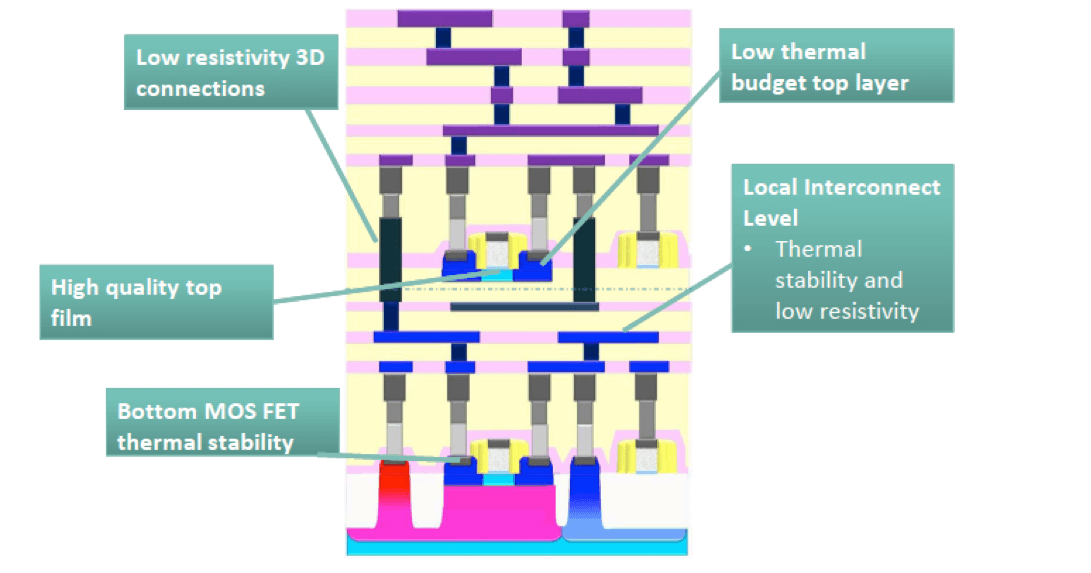
Today,the maximum thermal budget of in-situ doped source/drain bottom transistors has been quantified. For example, state-of-the-art FDSOI transistors exhibit no Ion/Ioff trade-off degradation, good thermal stability from junction (no dopant deactivation), mobility and EOT perspectives up to 550°C, and show improved thermal stability as compared to conventional technologies. The metal gate work-function to overcome the VT variation on short channel transistor and the silicide stability should still be improved to relax the top thermal budget limitation beyond 500°C. Laser anneal is a promising solution for optimizing the 3D layer stack (material and thickness) without exceeding the 500°C limit at the bottom level, while ensuring excellent top transistor performance.
Bottom layer thermal budget control and top layer low temperature process flow are key aspects for achieving the right balance between sequential higher integration with respect to advanced nodes performances. Additionally,to ensure a high quality of the top layer film, low-temperature molecular bonding has been chosen to preserve pristine wafer quality at the wafer scale. Finally, local interconnect levels have been introduced between the bottom and top transistors. 3D Interconnect low resistivity and thermal stability are also part of the process development in order to reach a good tradeoff between performance and contamination issues. Today, we have envisioned a realistic path for manufacturing 3DVLSI ICs using sequential integration.
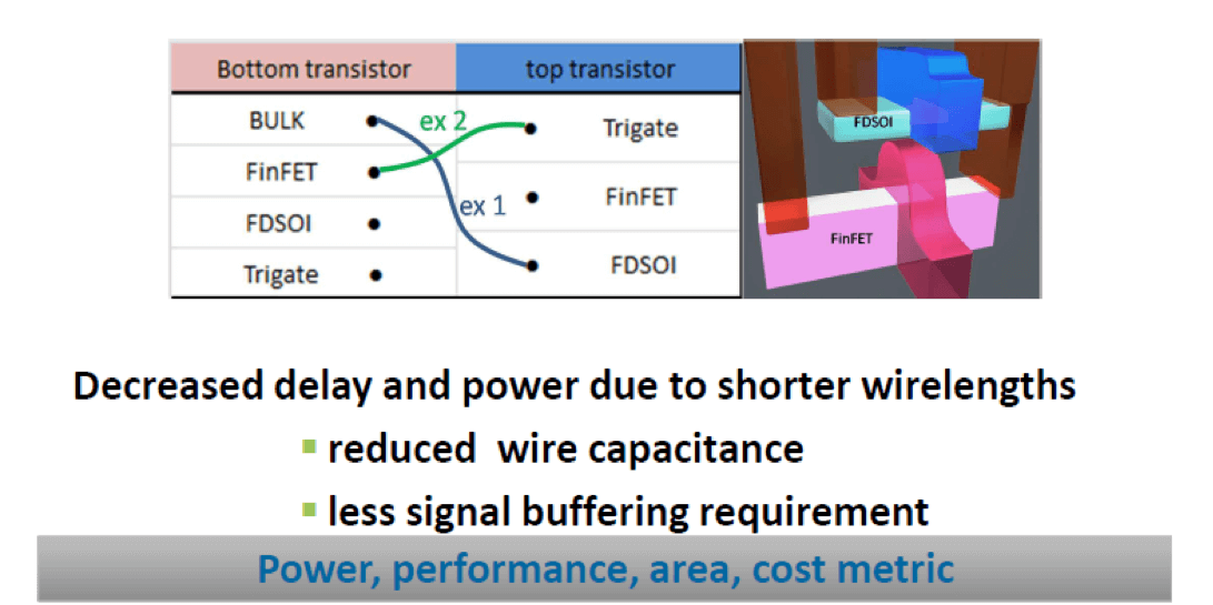
Addressing 3D Design challenges
The need for 3D is not only driven by device considerations but also by application requirements. To promote the new era of mobility and of big data, electronic equipment companies as well as individual consumers are looking for higher bandwidth, additional processing capabilities, and memory enhancements without trading-off for energy efficiency and cost competitiveness. Such heterogeneous system integration in package aims at mixing and matching different IP circuits on the same design flow for an optimized PPAC signature (Performance, Power, Area and Cost) (Figure 5).
3DVLSI technology has been the subject of many studies with various levels of complexity and accuracy. However, several milestones still need to be reached before planning tape-out trials with respectable confidence in term of PPAC gain. Moreover, 3D IC design requires new tools and methodology to obtain an optimized result. The high-level concept of 3DVLSI is clear, but the capability and the limitations have to be evaluated against a full set of parameters: number of device layers, number of interconnects levels, design rules, standard cells and memory blocks structures. Modeling and simulating complex devices interconnect schemes require simulations of the impact of thermal activity, stress, power, and clock distribution. Finally, several process options must be assessed and will require some accurate evaluation based on silicon data.
Current studies show that placing cells in a 3D architecture calls for a reliable netlist partitioning tool to split the 2D design into two 3D tiers. Placement quality is highly impacted by the results of this phase and requires specification of new design constraints, such as the number of interconnections allowed between tiers, power consumption of each tier, area ratio, or thermal constraints. In addition to this tool development, a new methodology is necessary. Actual place and route tools are only capable of handling 2D cell placement and require some modifications to perform well for 3D IC design. Even if some configuration tricks allow using them for some 3D trials with a few restrictions, tool upgrades will soon be mandatory to guarantee full integrity of the 3D-placed design to reach the same sign-off quality of results that we have for 2D IC.
The most promising technology or product, even if it exhibits best-in-class and unmatched features, is almost of no use without an ecosystem. For a disruptive ASIC technology such as sequential 3D integration to successfully address multiple applications, it is mandatory to build a very robust IP and Design ecosystem on top of reliable manufacturing and materials sourcing capacities. The involvement of best-in-class EDA suppliers and IP vendors will make the difference in collaboration of the development of foundation IP (new tools, standard cells library, memory compiler, etc.)
Conclusion
By design, LETI develops technologies ready for transfer to industry, and LETI is fully dedicated to support its customers in the maturation and the manufacturing implementation of its knowledge. In the case of CoolCube, LETI’s aim is to build a full ecosystem of partners to enable the industrialization of this technology at a rapid pace.
Recently, some world leading companies expressed interest in CoolCube technology to assess the feasibility of the concept. To expand the momentum around CoolCube, and to validate design and process assumptions through real prototyping products, the ecosystem will also require major manufacturing players to guarantee a large-scale industrial implementation. In parallel, other members of the value chain are invited to complete an ecosystem along the full added valued chain.
Authors
 Jean-Eric Michallet, VP Sales & Marketing CEA-LETI, MINATEC, Grenoble, France, joined CEA-LETI in 2013 after a 20-year career in technical and management positions at Altis Semiconductor and IBM Microelectronics. Prior joining CEA-LETI, he was technology transfer officer at University of Lyon (France). He was member of the board of Manesman Business Angels, an investment network for Hi Tech start-ups in Paris (France). Jean-Eric Michallet received and M.S degree in Microelectronics from ENSERG Institute (Institut National Polytechnique de Grenoble, France), an Executive MBA and a Master in International Management from Dauphine University Paris (France)/UQAM Montreal (Canada).
 Hughes Metras, VP Strategic Partnership, North America. CEA-LETI, is a visiting staff member at Caltech, Pasadena, California, USA. Prior his present position, Hughes Metras was VP Marketing and Sales, in charge of business development and strategic planning for CEA-Leti. He coordinated sales and marketing teams in the field of semiconductors (advanced CMOS as well as heterogeneous integration), imaging and photonics, biomedical technologies as well as telecommunications. Hughes Metras received an M.S degree in Signal Processing and Control Theory from Ecole Centrale de Marseille (France) and Executive MBA Business Management from University of Miami (Florida, USA).
 Maud Vinet, Head of Advanced CMOS Laboratory, CEA-Leti, joined Leti in 2001 as a device engineer. Her research has been focused on improving MOS transistors performance together with scaling its dimension. In 2009, she joined IBM Alliance in Albany as a Leti assignee to take part to the development of FDSOI. Within Albany state-of-the-art facilities, she extensively worked on device design and performance improvement of FDSOI devices. In 2013, she became Manager of the Advanced CMOS Laboratory in Leti. The laboratory pursues conventional scaling through improved electrostatics and transport properties. Focus is also put on alternative paths to conventional scaling either by stacking CMOS over CMOS in monolithic 3D integration or by adding beyond CMOS devices. Maud Vinet authored or co-authored about 120 papers (conferences and journals) and owns 40 patents related to nanotechnology.


Comments are closed.