Latest Posts
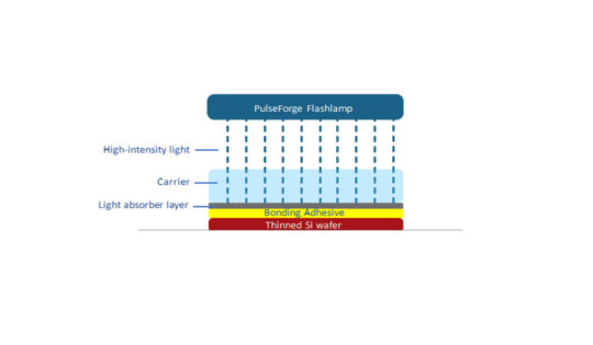
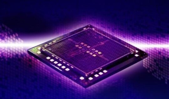
Adeia Selects PulseForge Photonic Debonding Equipment for Advanced Semiconductor Applications
Adeia Inc. (Nasdaq: ADEA), a leading innovator in research and development who has pioneered hybrid bonding in the semiconductor industry,...
EV Group and Fraunhofer IZM-ASSID Expand Partnership in Wafer Bonding for Quantum Computing Applications
EV Group and Fraunhofer IZM-ASSID partnership kicks off with the installation of EVG850 automated laser debonding system at the newly...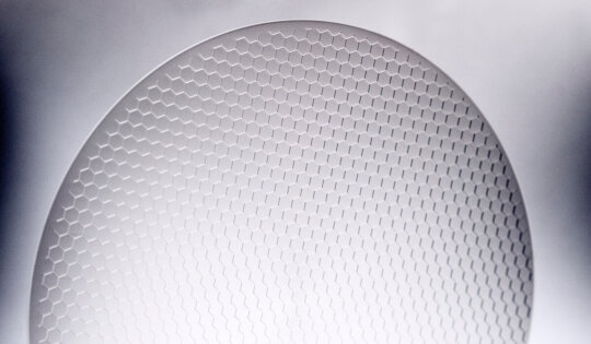
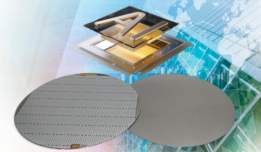
Carrier Wafers for Semiconductor and MEMS Manufacturing
As technology rapidly moves forward, the reduction of device and chip size is playing an important role in implementing as...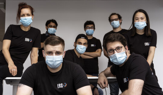
Social Distancing Spotlight: ERS Celebrates 50 Years of Thermal Solutions
50 years of providing specialized thermal solutions to the semiconductor industry is a significant accomplishment. It means your company is...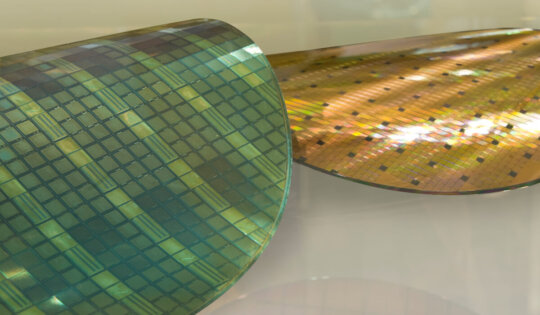
Temporary Wafer Bonding System Is Based On Electrostatics, Not Adhesives
Temporary wafer bonding is widely employed in semiconductor device fabrication and in semiconductor device packaging applications, particularly now that changes...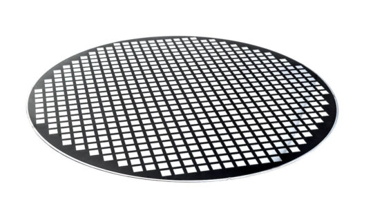
Temporary Bonding and Mold Process to Enable Next-Gen FOWLP
Temporary wafer bonding processes were initially developed for enabling three-dimensional (3D) stacked integrated circuits (ICs). For example, dies can be...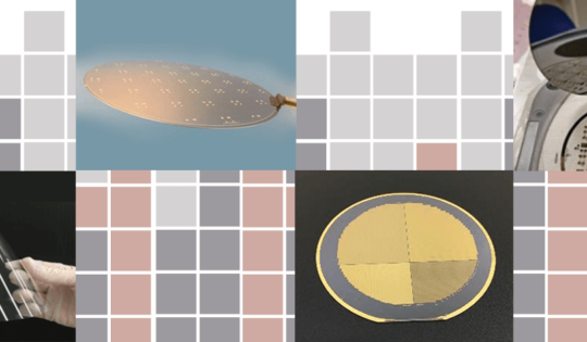
Mosaic Microsystems Wins Two SBIR Awards to Support Technology Development Initiatives
Mosaic Microsystems, a microelectronics and photonics packaging company providing thin glass substrates and through glass vias (TGVs) for next generation...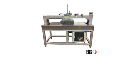
ERS electronic GmbH Takes the Lead in Fan-Out Panel Level Packaging Equipment Manufacturing
ERS electronic GmbH, the innovation leader in thermal management solutions for the semiconductor manufacturing industry, is taking the first ever...
Temporary Bonding and Debonding Technologies for Fan-out Wafer-Level Packaging
Fan-out wafer-level packaging (FOWLP) is a cost-effective way to achieve high interconnect density and to manage larger I/O counts within...
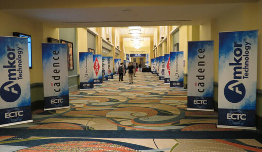
Impressions from ECTC 2017
Let’s start with the indoor rainstorm. I arrived at the Swan and Dolphin in Orlando just in time for the...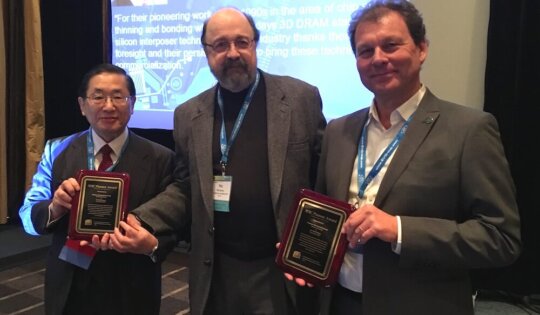
3D ASIP 2015: 3D Manufacturing Processes from the Early Days to the Present
For the first time since the 3D Architectures for Semiconductor Integration and Packaging (3DASIP) Conference was established, the organizing committee...
Advanced Packaging and 3D IC Market Driving Strong Growth for EV Group’s Automated 300mm Polymer Adhesive Wafer Bonding Systems
ST. FLORIAN, Austria, August 31, 2015—EV Group (EVG), a leading supplier of wafer bonding and lithography equipment for the MEMS,...
Executive Viewpoint: Providing A Golden Boat of Wafers
As 3D integration technologies become established in low volume manufacturing, the supply chain is gearing up to address high volume...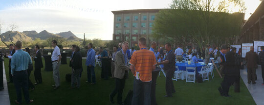
Addressing 3D IC Assembly Challenges at IMAPS DPC 2015
While we wait in the 3D IC holding pattern for products to go into high volume, processes continue to be...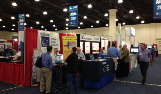
3D Technology Snapshots from IMAPS 2014
This year’s IMAPS International Symposium purported to have “the most interposer and 3D content under one roof.” I’m not sure...
Addressing 3D Integration Challenges: Designing Materials for a Complex Landscape
3D integration has created a complex landscape of many different package architectures and integration approaches that have diverse materials needs...
SEMICON West 2014: Supplier Updates for 2.5D and 3D Processes
SEMICON West 2014 brought its usual flurry of supplier announcements on new equipment and process improvements; but there weren’t as... SUSS MicroTec launches ELD300 Excimer Laser Debonder for 3D Integration
Garching, July 8, 2014 – SÜSS MicroTec, a leading supplier of equipment and process solutions for the semiconductor and related...