
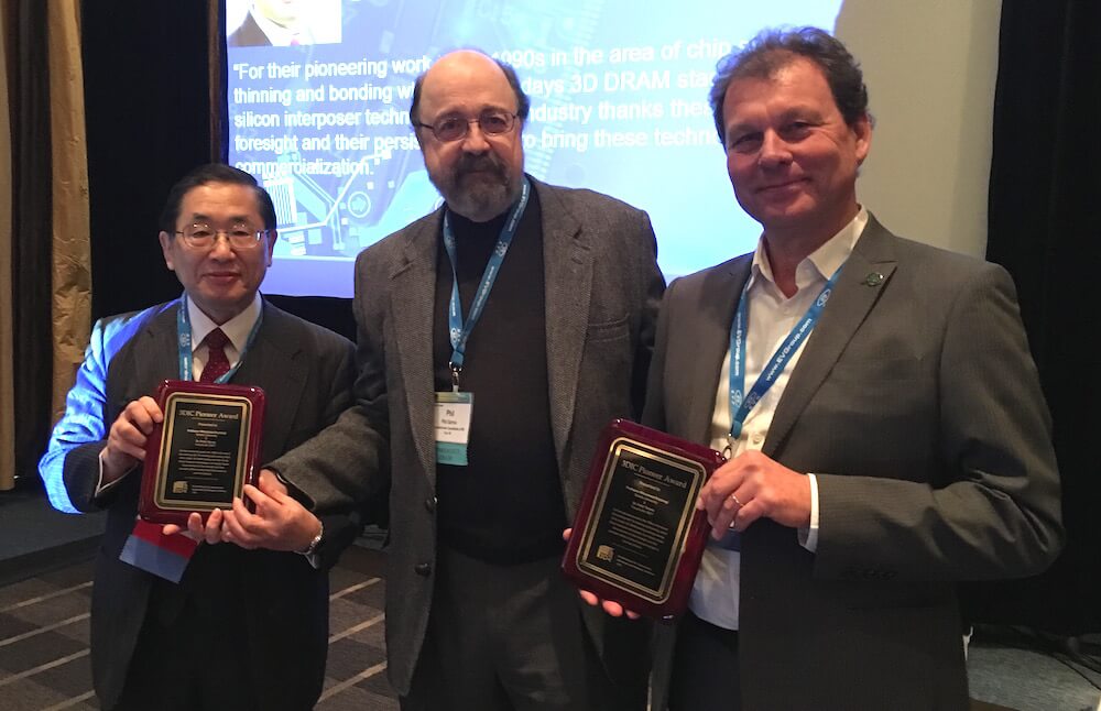
For the first time since the 3D Architectures for Semiconductor Integration and Packaging (3DASIP) Conference was established, the organizing committee decided to acknowledge the work of two researchers who were instrumental in developing the core processes that enabled 3D TSV development. In a brief ceremony, Dr. Phil Garrou presented 3DIC Pioneer Awards to Professor Mitsumasa Koyanagi, Tohoku University and Dr. Peter Ramm, Head of Department Heterogeneous System Integration, Fraunhofer EMFT “for their pioneering work in the 1990s in the area of chip stacking with TSV thinning and bonding, which lead to today’s 3D DRAM stacking and high-density silicon interposer technologies. Our industry thanks these pioneers for their foresight and their persistent efforts to bring these technologies to commercialization.” Each recipient provided the attendees with a trip down 3D memory lane through presentations of their work in this field as far back as 1985, which is when Professor Koyanagi started working on 3D versions of DRAM. I had no idea we had been working on this for so long.
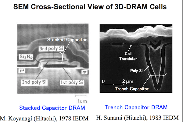
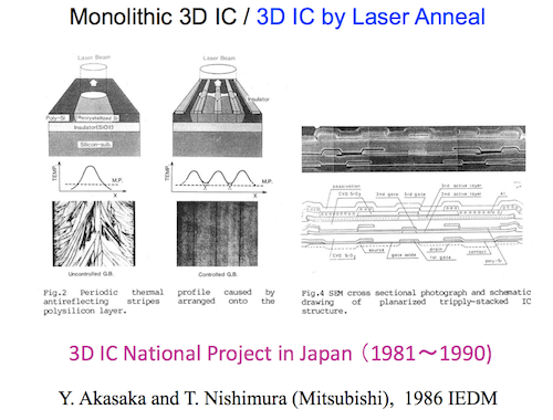
I was most intrigued by some of the earliest images Koyanagi shared. The first is early SEM images of what would later become Through Silicon Vias (TSVS). The second diagrams monolithic 3D IC concepts that he worked on between 1981 and 1990. “Perseverance” doesn’t begin to describe the efforts here.
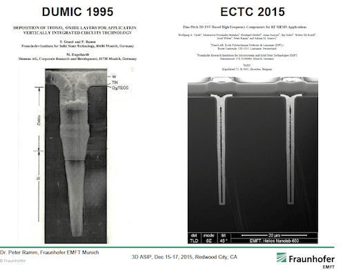
The history of 3D IC work at Fraunhofer Munich started in 1987, as part of various German and European Research Projects with ongoing support provided by Siemens and Infineon that occurred between 1987-1989, 1993-1996; 1993-2003, and now from 2007continuing through 2017. That’s 30 years devoted to developing processes for:
- 3D CMOS Devices
- Performance and thermal issues of 3D-ICs
- TSV processes
- Wafer thinning & thin die handling
- Wafer bonding
- Die-to-wafer stacking technologies (KGD)
- 3D integration technology is now entering a mainstream
- Memory stacks, memory/logic, … (high density TSVs)
- Heterogeneous sensor/IC integration (medium density TSVs)
- Choice of 3D process depends on
- Performance, TSV/pad pitch requirements
- Reliability requirements
Ramm said ongoing work is focused on TSV based RF-MEMS & RF-IC and highly reliable, ultra-low power 3D heterogeneous MEMS/IC systems. This image aptly illustrates what 10 years of work achieved in developing and fine-tuning processes for TSVs.
Understanding how much time and effort has gone into developing 3D processes that are appearing in products today makes commercialization of 3D TSVs that much more impressive. And we’re not done yet, as evidenced by presentations from several equipment suppliers on their continued efforts to further optimize processes to improve performance and reduce cost.
Day One of the conference featured a half-day tutorial on temporary bond/debond processes from research institutes, RTI International and CEA Leti; materials vendors HD Microsystems and Brewer Science; and equipment manufacturers, EV Group, TOK, and SUSS MicroTec.
I caught 3 of the six presentations, and got the distinct impression that the industry hasn’t completely figured this out yet. Or rather they have, but as Molly Hladik, Principal Applications Engineer, Brewer Science, explained to me, there’s not a one-size–fits-all solution. There are many and varied requirements depending on the application, and so what combination of material, process, and equipment suits one application may not suit another.
For example, from the materials menu, there’s a choice between thermoplastic, thermosetting, photosetting, and combinations. There’s also device-side release layer, or carrier side release layer materials to consider. For debonding, there’s mechanical debond, and laser-assist. Then there’s the matter of residue cleaning, and dicing tape. To complicate matters further, which process to choose depends on whether your process flow is for fan-out wafer level packaging (FOWLP), interposer integration, or 3D IC stacks for memory.

The tools must be configurable to a multitude of processes and material properties, and that’s a huge challenge. Not only that, but manufacturers must make all of these available to their customers. The good news is, all these equipment and materials vendors are reporting good yields when the right process is selected for the right application. It’s just a matter of knowing which combination suits your application, and which manufacturer has the capacity to deliver.
In one session devoted to equipment and metrology, there were three more process-focuses presentations by Markus Wimplinger, EV Group; David Butler, SPTS; and Rajiv Roy, Rudolph Technologies. (a fourth by Prashant Aji, KLA Tencor, was cancelled).
Wimplinger talked about permanent bonding for 3D ICs in high volume manufacturing. He said the main battles of taking wafer-to-wafer bonding to HVM have been alignment accuracy and throughput. Carefully controlled plasma activation is critical to the process.
Wimplinger focused on hybrid bonding, which bonds metal to a dielectric layer at room temperature, and is a preferred method for W2W bonding, as it is low cost and high-density solution. He gave a nod to Ziptronix as pioneers in the hybrid bonding space for its direct bond interconnect process (DBI).
According to Wimplinger, second-generation 3D backside illuminated (BSI) CMOS image sensors (CIS) use hybrid bonding without TSVs to form connections in the bonding interface. “Wafer bonding has arrived at the point in high accuracy and alignment where it enables high density interconnects, and is bringing 3D to the consumer market,” said Wimplinger.
David Butler, SPTS, stepped outside the company’s usual topic area of TSV etch process optimization to present a new process used for both FOWLP and 3D integration – plasma dicing. “We’ve heard a lot about large die today (700mm), but there’s far more being made with tiny die,” he said. Plasma dicing is driven by the need for more die, smaller die and smaller, thinner packages. It can reduce the widths between die, allowing for up to 80% more die per wafer.
Traditionally, dicing is done using a mechanical dicing saw. Alternatively, plasma dicing is a chemical process that is non-damaging, and results in stronger die post-separation. Butler said it doesn’t required water, there is no vibration, and there is no debris. He also said that process control via end point detection and notch prevention is critical to successful plasma dicing, and is something SPTS’s system can do.
Lastly, Roy talked about Rudolph Technologies latest advancements in lithography, inspection, and software to address the need for finer line/space requirements coming with high density FOWLP. Two areas affecting final yield has been die shift and wafer warpage. The company has developed lithography processes to correct both. They’ve also introduced an industry first: high-speed fluorescent imaging for semiconductors. Roy explained that the variety of materials used in FOWLP requires more than just bright field imaging to detect possible defects. They’ve discovered that by combining fluorescent and bright field imaging, they can detect more residues.
With FOWLP and 3D ICs becoming commercialized and approach volume manufacturing, it’s clearly worth the effort to continue to improve processes to increase yields and ultimately lower costs. ~ F.v.T.


