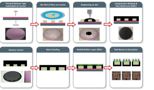
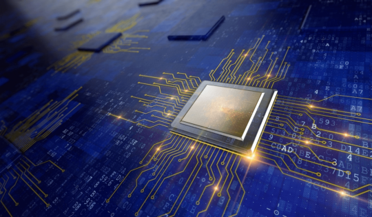
As next-generation High-Density-Advanced-Packaging (HDAP) designs become more common, PCB designers and engineers are looking to system-level co-design to tie multi-substrate...
Traditionally, MCMs (Multi-Chip-Modules) were a way of integrating several ASICs, or ASICs and memory, into a lower-cost, smaller form-factor, robust...
Today’s SoCs, multi-core CPUs and GPUs with their high performance, high bandwidth interconnect interfaces put demanding challenges across the entire...
Fan-out wafer-level packaging (FOWLP) is an emerging type of high-density advanced packaging (HDAP) technology in the semiconductor industry that is...
The industry standard interconnect technology for fine-pitch 2.5D assembly and 3D stacking is thermocompression bonding of solder capped μbumps. This...
Consumer electronics designers continue to demand thinner and lighter packages while devices increase in functional complexity. The Fan-Out Wafer Level...
Organic paper, particularly cellulose-based paper, efficiently served in previous eras as an engineering material. In the Tang dynasty, soldier armors...