
The growing demand for semiconductors, from the cloud to the edge, from artificial intelligence (AI) to 5G communications, has exceeded the capabilities of traditional silicon scaling. In the “More than Moore” era, performance requirements for leading-edge semiconductor devices demand extremely fine pitch (<10µm, or even <1µm) interconnection in semiconductor packaging and heterogeneous integration. Direct copper interconnection has emerged as the technology of choice in the semiconductor industry for fine-pitch interconnection, with significant benefits for interconnect density and device performance.
Hybrid bonding, as a low-temperature direct copper bonding technology, in particular, will become widely adopted for a broad range of high-performance semiconductor devices in the years to come. It will enable the continued growth of economically viable power-efficient computing, for example, utilizing chiplet-based heterogeneous integrated packaging technologies.
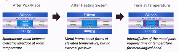
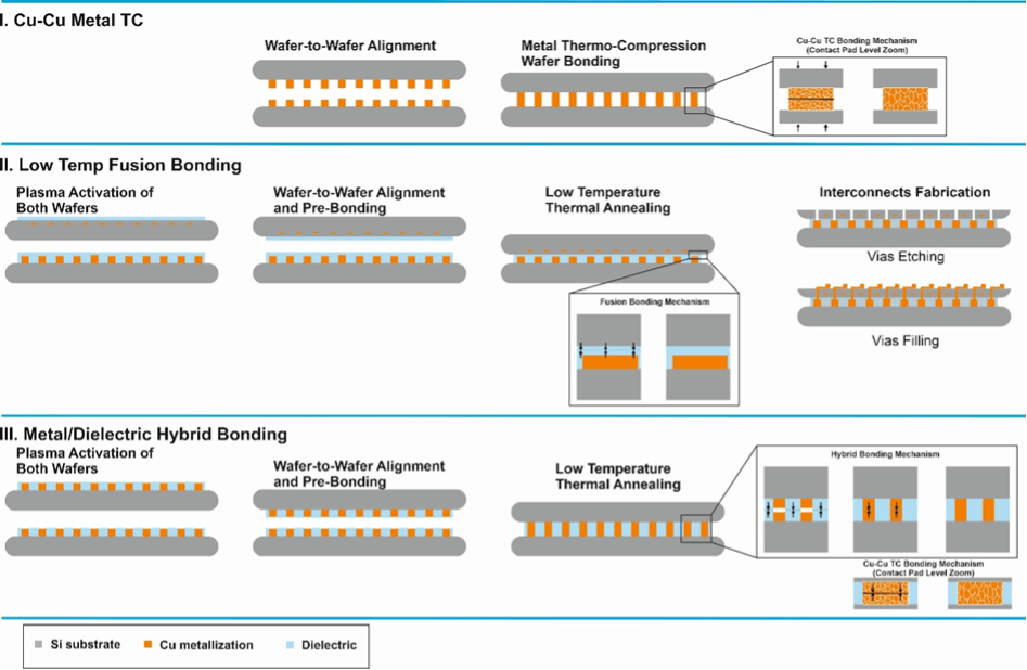
Hybrid bonding technology is an all-solid-state joining technology (Figure 1) that forms a spontaneous dielectric-to-dielectric bond at room temperature and then establishes a metal-to-metal connection (usually Cu-to-Cu bond) by a low-temperature batch annealing process (150 – 300oC), potentially enabling sub-micrometer bonding pitch.
Various applications, including CMOS image sensors (CIS), computing, memory, and photonics, will drive the proliferation of hybrid bonding to provide improvements in power, performance, area, and cost (PPAC). As hybrid bonding technology transitions from the lab to the manufacturing floor, the maturity of the process technology and the robustness of the eco-system are critical factors for industry-wide adoption of the hybrid bonding technology to enable product applications.
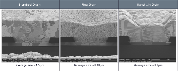
Extensive development work over the years has enabled stable manufacturing processes with acceptable yield. Materials development and equipment technologies have been optimized for cleanliness, alignment accuracy, throughput, and yield, along with metrology and characterization tools. Thin wafer handling, warpage, flatness, and dishing control, are some of the critical process attributes that need to be optimized for volume manufacturing. Dielectric materials and electroplated copper microstructures (Figure 2) are also important factors for process yield, cycle time, and bonding integrity. Reliability testing and performance characterization (electrical and thermal) have offered confidence for product adoption. Design methodologies can enable the optimum configurations to take the most advantage of the technology.
Direct Copper Interconnection for Advanced Semiconductor Technology
 The forthcoming book, “Direct Copper Interconnection for Advanced Semiconductor Technology”, offers a comprehensive review and in-depth discussions of these key topics in this critical new technology. It features chapters contributed by many industry experts, including several members of the 3D InCites community.
Chapter 1 reviews the evolution and the most recent advances in semiconductor packaging, leading to the requirement for extremely fine-pitch interconnection. Chapter 2 reviews different technologies for direct copper interconnection, with advantages and disadvantages for various applications.
Chapter 3 offers an in-depth review of the hybrid bonding technology, outlining the critical processes and solutions. The development history of the technology, bonding mechanisms, and processes (including bonding layer fabrication, wafer thinning and dicing, die and wafer preparation, wafer-to-wafer bonding, die-to-wafer bonding, and heated anneal), are discussed in detail.
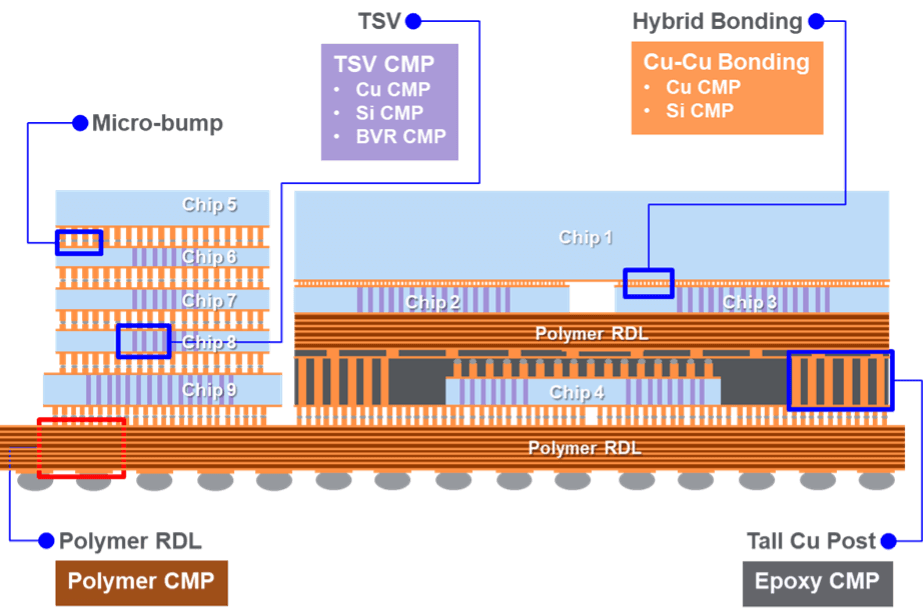
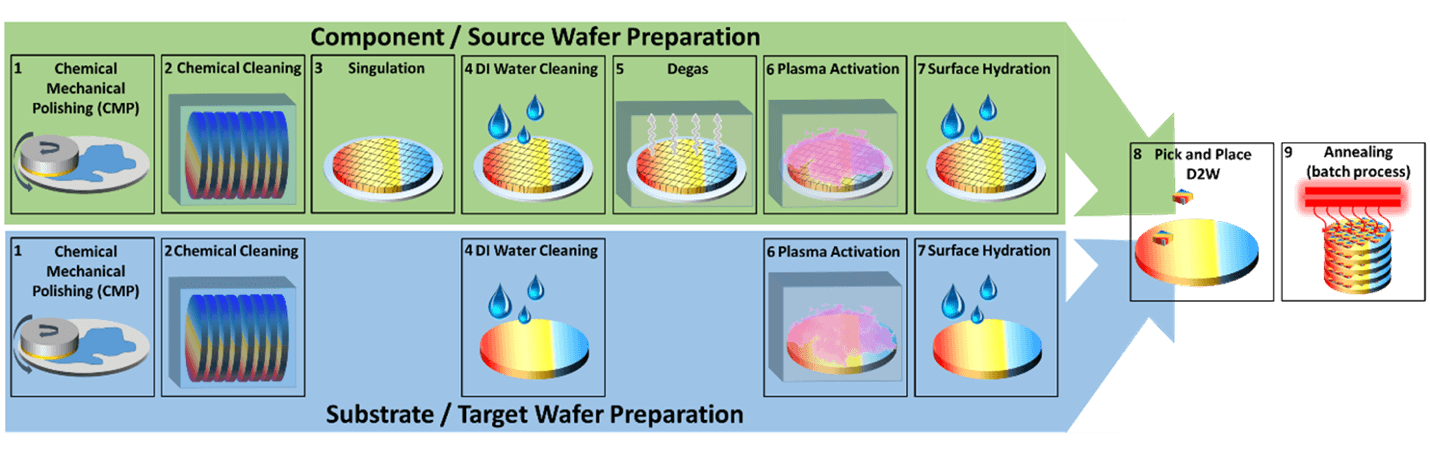
The area of materials (including temporary and permanent wafer bonding materials and dielectrics) for hybrid bonding is covered in Chapter 4, followed by several chapters that are focused on critical process steps and equipment for copper electrodeposition (Chapter 5), chemical mechanical planarization (CMP) (Chapter 6) (Figure 3), wafer bonding (chapter 7) (Figure 4), and die bonding (Chapter 8) (Figure 5). Both die-to-wafer (D2W) and wafer-to-wafer (W2W) scenarios are discussed, in terms of the process technology, equipment, and product applications.

In addition, metrology and testing are also addressed throughout the chapters. Business, economic, and supply chain considerations are discussed as related to the product applications and manufacturing deployment of the technology, and the current status and future outlook as related to the various aspects of the eco-system are outlined in the relevant chapters of the book.
The initial product adoption of the hybrid bonding technology has clearly demonstrated the significant benefits of product performance improvements, including interconnect density, bandwidth, energy efficiency, thermal performance, signal integrity, and reliability. The maturity of the process technology will lead to meaningful yield improvements over time, enabled by a robust ecosystem.
As the hybrid bonding technology and the eco-system mature, more interesting applications will emerge to exploit the further scaling in interconnection density and bandwidth, especially in the era of AI computing, for enhanced computing and memory capabilities. 3D V-Cache and 3D NAND, High Bandwidth Memory (HBM), DRAM multi-layer stacking, and DRAM-to-logic bonding, are some of the applications to meet the demand for higher bandwidth and higher energy efficiency. Silicon photonics is yet another exciting application to utilize the high bandwidth, high power efficiency and low loss of optical I/O, with superior performance from electrical-optical interconnects in the EIC/PIC chiplet integration enabled by hybrid bonding. Heterogeneous integration applications involving III-V semiconductors and glass interposers will also emerge to take advantage of hybrid bonding.
Hybrid bonding is a critical enabler of the integrated chiplet architecture, which will become pervasive for high-performance semiconductor devices. It is expected that the broad adoption of the hybrid bonding technology will enable further scaling in interconnect density (1M/mm2), over the next few years. The combination of high interconnect density with superior performance (electrical, thermal, and reliability) makes hybrid bonding a compelling technology for advanced semiconductor devices.
As the technology further matures and the manufacturing cost decreases over time – enabled by a robust eco-system and integrated cluster tools (ICT), it will proliferate from foundries to OSATs, for a broader range of products – including RF, automotive, AR/VR, microLED, and others. Front-end processes and back-end processes will be further integrated, and the boundary between foundries and OSATs will be blurred even further over time.
The time has come for hybrid bonding for advanced semiconductor technology. For further information, please contact Dr. Dongkai Shangguan at dongkai@thermengr.com.
References
G. Gao and L. Mirkarimi, “Hybrid Bonding Process Technology”, in: “Direct Copper Interconnection for Advanced Semiconductor Technology”, D. Shangguan (editor), CRC Press, 2024.
B. Buckalew, “Copper Electrodeposition for Advanced Packaging & Hybrid Bonding”, in: “Direct Copper Interconnection for Advanced Semiconductor Technology”, D. Shangguan (editor), CRC Press, 2024.
B.J. Brown, E. Mikhaylichenko, J. Tang, J. Qian, and Y-C. Yang, “Planarization for Advanced Packaging and Hybrid Bonding”, in: “Direct Copper Interconnection for Advanced Semiconductor Technology”, D. Shangguan (editor), CRC Press, 2024.
V. Dragoi, T. Uhrmann, and P. Lindner, “Permanent and Temporary Wafer Bonding”, in: “Direct Copper Interconnection for Advanced Semiconductor Technology”, D. Shangguan (editor), CRC Press, 2024.
J. Abdilla and S. Schmid, “Die to Wafer Hybrid Bonding for Direct Copper Interconnection”, in: “Direct Copper Interconnection for Advanced Semiconductor Technology”, D. Shangguan (editor), CRC Press, 2024.