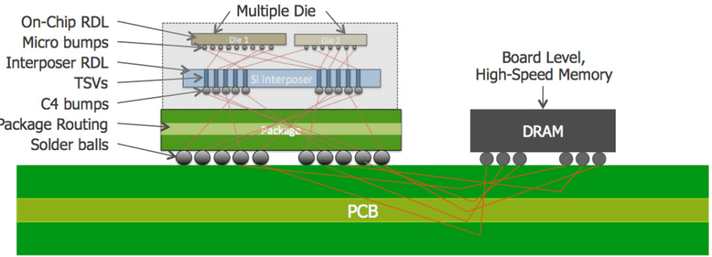
![]() As next-generation High-Density-Advanced-Packaging (HDAP) designs become more common, PCB designers and engineers are looking to system-level co-design to tie multi-substrate visualization, planning, and optimization, into a complete multi-board design. Co-design methodology allows design teams to plan and optimize I/O and connectivity from a chip, through multiple packaging scenarios, and on to printed circuit boards for complete system-design success
As next-generation High-Density-Advanced-Packaging (HDAP) designs become more common, PCB designers and engineers are looking to system-level co-design to tie multi-substrate visualization, planning, and optimization, into a complete multi-board design. Co-design methodology allows design teams to plan and optimize I/O and connectivity from a chip, through multiple packaging scenarios, and on to printed circuit boards for complete system-design success