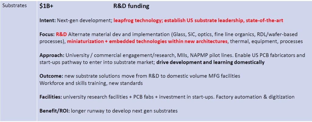
IMAPS Reshoring Part 2: High-Density Build-Up Substrate Discussions
Picking up where we left off in IFTLE 564, the second discussion session was supposed to be focused on the availability of high-density build-up substrates (HDBU) and where we stand in moving production onshore.
Jan Vardaman of TechSearch International announced that a decline in PC, consumer, and other markets eased the shortage of build-up FC-BGA substrates; and with the planned capacity expansion created an oversupply situation. In other words, the shortages that we have faced in the supply chain for more than a year are now over. Unfortunately, this led to the industry returning to the practice of pushing down on prices, reducing gross margins for substrate suppliers. As a result, current Asian suppliers are not seriously considering building plants in the US under such falling price conditions. Vardaman indicated that current US suppliers like TTM, Calumet, and Greensource were currently not capable of meeting Asian technology capability, pricing, or delivery time.
According to Vardaman limitations preventing new substrate suppliers from locating in the U.S. includes:
- Defense volumes are not sufficient to operate production lines (even with incentives) thus it’s not possible to generate sufficient volume to run operations.
- Major high-performance computing (HPC) customers want to use the existing supply chain in Asia (including assembly)
- Lack of skilled workforce – engineering and operators
- No sustainable business model for high volume in U.S. production
The IPC’s Matt Kelly, unfortunately, spent more time trying to convince the audience that advanced packaging was important than focusing on the details of HDBU and high-density interconnects (HDI), which after all is the focus of the IPC (Institute of Printed Circuits). His presentation on IPC’s take on advanced packaging was certainly not what I was looking for in this discussion session. It was obvious that seeing where the leading edge is going, the IPC wants to be much more active in the advanced packaging arena. Figure 1 focused on what was needed in the area of the substrate.
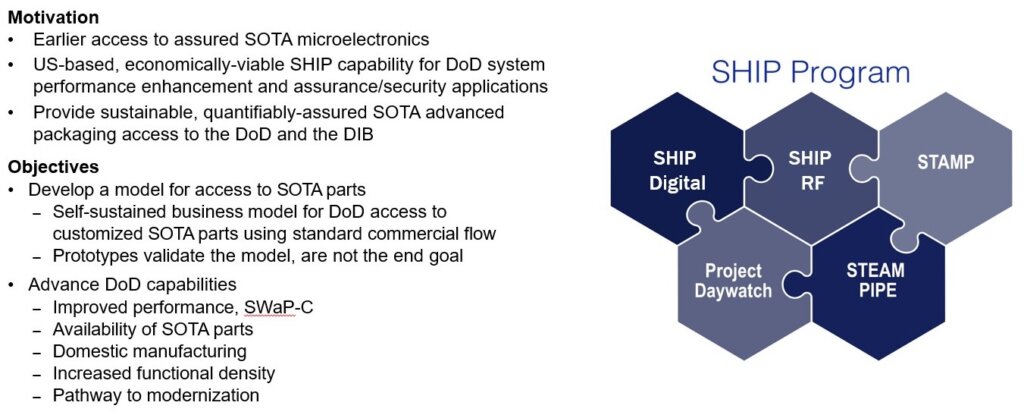
SHIP Update
Brian Olson, SHIP RF Technical Manager for Advanced Packaging and Test Technical Execution Area in the Office of the Under Secretary of Defense for Research & Engineering updated the audience on the State-of-the-art Heterogeneous Integrated Packaging program [SHIP]. The SHIP program is described in Figure 2.
As we have noted before in IFTLE, SHIP digital is led by Intel, and SHIP Rf is led by Qorvo. SHIP digital currently consists of four multi-chip packages (MCPs) as shown in Figure 3.
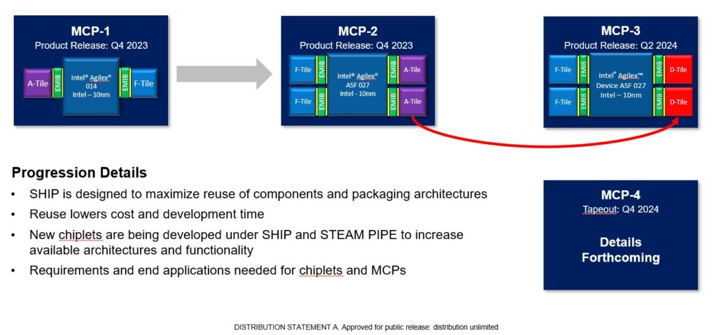
SHIP MCP-1
- Fabricated at Intel Corporation and features three silicon die connected using embedded multi-die bridge (EMIB) packaging technology
- Brings components closer together, reducing latency and power while increasing signal processing ability
- Through SWAP savings, MCP-1 will deliver:
- Unprecedented spectral agility
- Enhanced signal processing
- Lower power consumption
- Improved thermal management
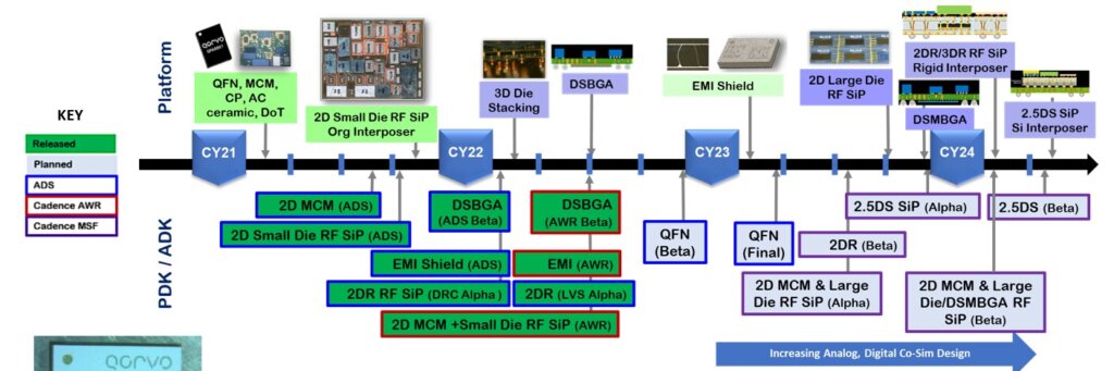
SHIP Rf
The roadmap for the Qorvo SHIP Rf program is shown in Figure 4.
![[err-ad-fallback-title]](http://www.3dincites.com/wp-content/plugins/a3-lazy-load/assets/images/lazy_placeholder.gif)
Stimulating Transition for Advanced Microelectronics Packaging (STAMP)
- Stimulate SHIP device transition by working with the DIB to translate warfighting capabilities and align devices to an existing DoD Program Office
- Provide SHIP hardware for DIB to utilize in existing relationships with Program Offices
- Accelerate tech adoption using a cost-sharing model aimed to buy down risk for Program Offices
- This will allow broader DIB to utilize SHIP devices and identify where MCPs can enable modernization
- USG will engage in cost-sharing to reduce transition risk and promote the accelerated transition
Strategic Transition of Microelectronics to Accelerate Modernization by Prototyping and Innovating in the Packaging Ecosystem (STEAM PIPE)
Through chiplet and advanced packaging prototyping:
- Develop and build chiplets for relevant DoD applications
- Establish and grow chiplet ecosystem maximizing reuse
- Develop and build new packaged prototypes with high probability transition path into DoD systems
- Continue to mature domestic packaging capability
DAY WATCH
Focusing on MCP-1
- Address perceived risk associated with inserting EMIB solution into DoD systems
- Inform DIB about MCP reliability in relevant DoD environments, reducing transition risk
For all the latest on Advanced Packaging stay linked to IFTLE………………………………