

The week of July 10th IMAPS held its now annual reshoring conference jointly with the IPC. The General Chair of the meeting was Darren Crum, Office of the Undersecretary of Defense for Research and Engineering – Advanced Packaging Lead and the Technical Chair was Brandon Hamilton, Program Manager for Microelectronics Packaging for BAE Systems.
We discussed the overall program agenda of the restoring conference in detail in IFTLE 559. As we discussed, attendance was set up for US / Canadian citizens only and included key members of the government agencies supporting advanced packaging reshoring, and the Defense Industrial Base (DIB), i.e users of the advanced packaging technologies and US-based outsourced semiconductor assembly and test service providers whose technologies are available to the DIB and the DoD. Presentations were by invitation of the committee.
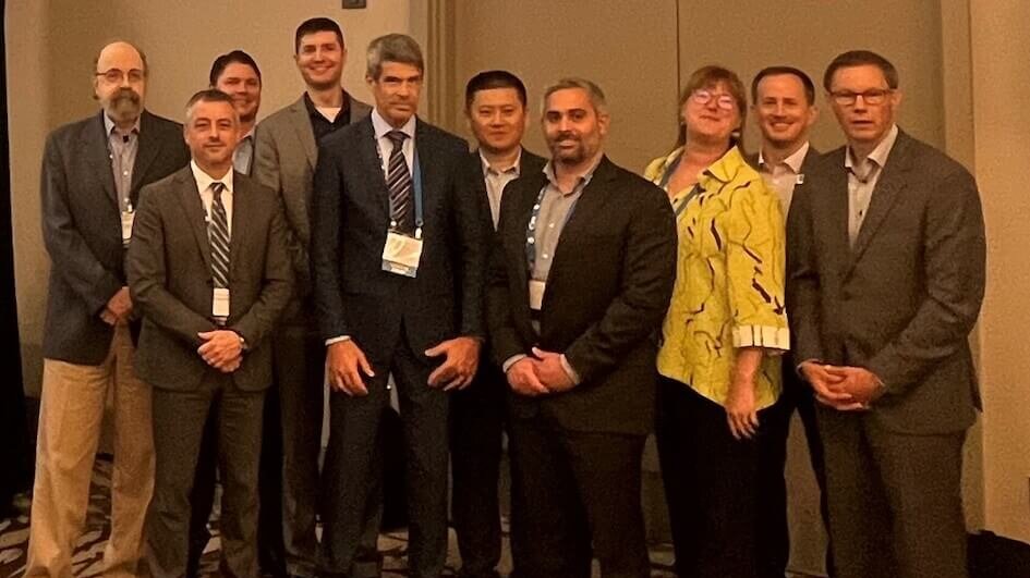
The organizing committee for this workshop is shown above and included (from L to R): From left to right: Philip Garrou IFTLE; Brandon Hamilton, BAE Systems; Steven Dooley, Air Force Research Laboratory; David Shahin, Northrup Grumman Advanced Systems; Darren Crum, US Navy; Tony Trinh, Mercury Systems; Christopher Riso, Booz Allen Hamilton; Helen Phillips, NGC; Brian Schieman, IMAPS; and Matt Kelly, IPC. (Not available for the photo were James Will, SkyWater Technology Foundry; Ted Tessier, Integra; and Jason G. Milne, Raytheon.
On Monday afternoon we held two discussion groups on topics that we felt needed open group discussion: Namely chiplets and advanced substrates. The former was headed up by John Park of Cadence and Bob Patti of NHanced Semiconductor, and the latter by Jan Vardaman of TechSearch International, Inc. and Matt Kelly of the IPC.
The reshoring conference format was a new concept proposed by General Chair Crum, who suggested we not have the traditional panel sessions during which the panelists use up most of the time focusing on their pet topics and the audience asks very few questions. We sought to have two experts lead the conversation, but the topics discussed over these two-hour sessions were driven by the audience who had a chance to ask questions, challenge concepts and clarify their understanding of these topics.
Chiplets
Without question, the concept of chiplets still appears to be a controversial topic that part of our community still does not fully understand. We asked John Park of Cadence, an accepted authority in the area to lead off the discussion with a few introductory slides to set the stage for questions. Bob Patti of NHanced then followed by taking questions from the audience. The allotted two hours flew by and included lots of interesting discussions.
Looking at some chiplet basics again:
The IEEE Electronic Packaging Society (EPS) has offered this discussion/definition in response to confusion in the industry:
“The naming of new technologies can be difficult and often inaccurate. Over time, standards are developed and language becomes aligned.
The cost of leading-edge nodes, combined with the lack of scaling of significant design blocks (ex: analog) and die sizes reaching reticle size, is driving disaggregation (splitting up) of chip functions into their best price/performance nodes requiring new technologies to interconnect these functions.
We are voicing our support in naming these small IP blocks “chiplets”. It is not a perfect name but fits into our vernacular well and is gaining acceptance in our industry. Here is our definition of “chiplet”, and what it is not.
Chiplet is not a package type, it is part of a packaging architecture. Thus, in large and complex chip designs the design is subdivided into functional circuit blocks, often reusable IP blocks called “chiplets”, that are manufactured and recombined on high-density interconnect.
Historically, the need for multiple chips to deliver a specific function was driven by the reticle limit which dictated the maximum size of a chip possible to be fabricated. Designs that exceeded the reticle limit were split up into smaller dies to be manufacturable. As technology continued to enable increased integration, multiple dies were merged into single, more complex ICs. Thus, the origin of the term “system on a chip” or SoC.
More recently, economics has caused a reversal of that trend. As the industry moves to smaller process nodes, costs for yielding large dies increase. The desire to move to a chiplet-based design has been driven by the increasing cost of manufacturing devices on leading-edge process nodes. Compared to a 250 mm² die fabricated on a 45nm process, a 16nm process more than doubles the cost/mm² and a 7nm process further doubles that to 4x the cost per yielded mm². Moving to the 5 nm and even 3 nm nodes, is expected to make this even worse.
The chiplet solution can be used to ease the economics of manufacturing such chips, with large numbers of transistors, at state-of-the-art nodes. In chiplet-based design, the chip is broken down, by function, into multiple smaller chiplets and only the chiplets that require the latest node are made in that node.
Some envision, that in time, the greater use of chiplets will drive the package to become the new SoC, and chiplets become the new “IP”. However, for this to be viable across packaging companies, there must be standard/common communication interfaces between chiplets. There are several solutions today, but standards must be chosen.”
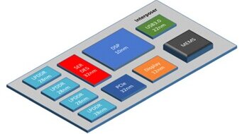
Thus, chiplets are an alternative design methodology to monolithic chips. A single chiplet design would typically have a single function, be operationally dependent on other chiplets, and be reusable across a range of products and product generations. An example is shown in Figure 1.
A major advantage of chiplets over monolithic designs is that smaller chips are higher yielding. One of the fundamental disadvantages of using chiplets is the need for additional on-package interconnects to allow the chiplets to communicate with each other. This extra interconnect can reportedly increase the amount of silicon by 10% over a monolithic design. So, the benefits of cutting up a large chip into smaller chips have to be balanced against the additional costs of the extra area taken up by the interconnects and extra packaging costs.
One easy way to look at all of this is: If you think you have a chiplet module but cannot identify the communication protocol that is used to communicate between the chiplets, you probably DO NOT have a chiplet based module.
Most of the audience agreed that to truly become a pervasive technology that offered a library of chiplet functions from which designers could create new circuits, standard communication protocols are absolutely necessary. The industry must be able to mix and match chiplets from different vendors into the same modules.
Most in the audience believed that the “standard communication protocol “winner would eventually be UCIe. A group of industry players, led by AMD, Arm, Intel, Samsung, and TSMC formed the Universal Chiplet Interconnect Express (UCIe) created the UCIe standard with the goal of “…standardizing die-to-die interconnects between chiplets with an open-source design, thus reducing costs and fostering a broader ecosystem of validated chiplets”. The UCIe standard, released in March of 2022, aims to become just as universal as other connectivity standards like USB and PCIe. It is key that all of the leading foundries will adopt this tech.
For a more detailed look at UCIe IFTLE suggests the article in Tom’s Hardware.
UCIe is a layered protocol with a physical layer and a die-to-die adapter. The physical layer can consist of different types of current packaging options including standard 2D packaging and more advanced 2.5D packaging like Intel’s EMIB or TSMC’s interposer-based CoWoS, and fanout interposer approaches, like ASE’s FOCoS-B. The UCIe standard will reportedly expand to 3D packaging interconnects in the future.
A protocol layer runs on top of the physical layer, and the initial specification relies upon PCIe or the open Compute eXpress Link (CXL ) protocol. The PCIe protocol provides wide interoperability and flexibility, while CXL can be used for more advanced low latency/high throughput connections, like memory, I/O, and accelerators such as GPUs and ASICs. While the specification begins with PCIe and CXL as the current protocols, it hopes to expand to include other protocols in the future.
Intel had previously used its Advanced Interconnect Bus (AIB) protocol for its EMIB packaging technology. While Intel made AIB open-source and royalty-free, it didn’t gain much industry traction. Intel has since announced that while it will continue to support current AIB implementations, it will stop all further development and migrate to UCIe over the next few years.
For all the latest on Advanced Packaging stay linked to IFTLE…………………………………….

