
In a recent report, Semianalysis examines the migration from planar to finFET to nanosheet to complementary FET to 2D transistor designs. Since IFTLE has always preached that one must understand where IC transistor technology is going in order to be able to predict advanced packaging changes, this report is certainly worth taking a closer look at.
Background

For many generations, the switching speed of planar transistors could be increased by shrinking the gate length. “Straining” the silicon channel was also found to increase the switching speed. Electron mobility reportedly improves by 70% in strained channels, leading to transistor switching speed increasing by 35%.
A further development that allowed continued scaling of planar transistors was “high-k gates”. Intel’s 45 nm process in 2007 used a hafnium-based dielectric layer producing a “high dielectric constant” or “high K” gate. The rest of the industry followed three years later.

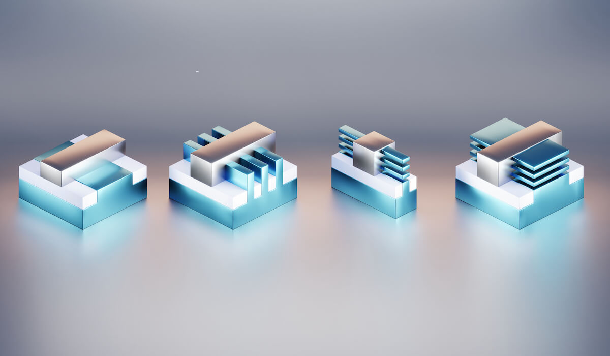
As transistor dimensions continued to shrink, the gate lost the ability to properly control the flow of current in the channel, i.e the planar transistors displayed significant “short channel” effects. Below the 28nm node leakage current became excessive. The industry shifted to “3D” transistors, known as FinFETs where the gate wraps around the channel on three sides of a silicon fin. This allows for greater control of the current flow through the transistor. FinFET transistors have significantly faster switching times than planar transistors. Intel moved into production with FinFET at the 22nm node, and foundries like TSMC ramped up the FinFET at 16nm.

Due to the limit of how thin/high fins can be made as well as how many fins can be placed side by side, another evolution was necessary. These “Gate-All-Around (GAA) ” transistors use stacked horizontal “nanosheets” so that the gate surrounds the channel on all 4 sides. This increases the drive current and overall performance of such transistors. Samsung began using GAA in its 3nm process in 2022 with high volume expected in 2024. Intel has GAA on its roadmap at their 20A process node (products shipping in 2025). TSMC has GAA with their N2 process node in 2025 / 26.
To continue beyond 2nm, GAA will also require new transistor channel materials for the nanosheets. This is because the electron mobility in bulk materials like silicon and germanium drops significantly < 5nm. Semianalysis predicts that “Perhaps the best family of materials to address these challenges is 2D materials”.
TMDs Are Promising for Nanosheets
For instance, IMEC’s roadmap introduces a complementary FET (CFET) solution, in which the n and p channels, based on monolayer transition metal dichalcogenides such as WS2 or MoS2 are stacked.
2D materials are crystalline solids consisting of a single layer of atoms. The most well-known 2D material is graphene, an allotrope of carbon consisting of a single layer of atoms arranged in a hexagonal lattice. But, despite its high electron mobility, without a bandgap, graphene can’t be used as a semiconductor material. Carbon Nanotubes are 1-dimensional materials but remain difficult to manufacture after 30+ years of intense R&D.
The most promising 2D materials for next-gen nanosheets come from the “transition metal dichalcogenides (TMD)” including Molybdenum disulfide (MoS2), Tungsten disulfide (WS2), and Tungsten Diselenide (WSe2). Such materials reportedly have the desired combination of bandgap + mobility required for < 5nm channel thicknesses. 2D materials are often grown via chemical vapor deposition (CVD) or atomic layer deposition (ALD). While direct growth of 2D materials on silicon is preferred, thus far, it has been difficult to achieve a low-temperature, high-quality growth solution. While ALD allows for lower temperatures than conventional metalorganic CVD or MOCVD, throughput remains slow. Since 2D growth is often done at high temperatures (>600° C) on optimized substrates like copper or sapphire, a transfer step is required to move the 2D material to the final silicon wafer.

Semianalysis reports that today’s 2D material transfer methods are sufficient for some applications/devices like sensors but cannot be used for CMOS fabrication in terms of quality, throughput, and contamination. Looks like an opportunity here for the right technology!
While TMD-based devices are promising, there is a fundamental issue on TMD growth methods. Transfer-based methods leave polymer residues, while direct growth on oxide with MOCVD results in a variety of defects, most notably organic contaminants and sulfur vacancies.
Defense Production Act Title III Presidential Determination for Printed Circuit Boards and Advanced Packaging Production Capability
On March 27th the President authorized the use of the Defense Production Act to support the nation’s domestic Printed Circuit Boards (PrCB) and Advanced Packaging industrial base.
This allows the DoD to utilize its Defense Production Act (DPA) Title III authorities to invest in advanced microelectronics capacity and ensure the production of state-of-the-art integrated circuits in the United States.
This executive order prioritized the need to support and advance the domestic PCB and advanced packaging industrial base to address strategic vulnerabilities to U.S. military readiness and challenges to American economic competitiveness.
For all the latest in Advanced Packaging stay linked to Insights From the Leading Edge ( IFTLE)…


