

Last year (IFTLE 512) we discussed the SKC formation of the US subsidiary Absolics, and its glass core substrate manufacturing capabilities. In recent news, Applied Materials recently announced that it will acquire $39 million worth of Absolics shares.
Absolics is issuing new shares to raise capital to expand its glass core substrate production facilities. Of the 130,000 new shares, SKC and AMAT will reportedly acquire 90,000 and 40,000 shares, respectively.
According to the Korean filing, “The new funding will be spent on Absolics’ new chip glass substrate plant in the US,”. SKC broke ground for the construction of the 12,000-square-meter production facility, located in Covington, Georgia, in November 2022. Production is expected to start in the second quarter of 2024.
Samsung Advanced Packaging Team
Samsung Electronics, the world’s biggest memory manufacturer, has officially set up a new team dedicated to developing advanced chip packaging solutions within its semiconductor business.
Samsung Electronics Device Solutions (DS) division reportedly created an advanced package team in the Test & System Package (TSP) department. TSP is responsible for the whole semiconductor packaging solution development and manufacturing process from solution development to mass production, testing, and product shipping.
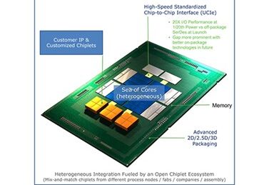
Apple and Tesla, major chip customers, increasingly opt for customized manufacturing orders for their self-developed chips and ask foundry companies to package chips with different functions in one package for better performance.
Samsung Electronics expects its chiplet technology to play a key role in meeting customer demands for high-performance chips, and the new advanced chip packaging solution team is expected to help the company better prepare for big changes to the chip packaging business.
The move is seen as an effort by Samsung Electronics to create synergy between memory and foundry businesses.
CHIPS Update
NIST held a meeting of its Industrial Advisory Committee (IAC) in early December to update the committee on the progress of the Creating Helpful Incentives to Produce Semiconductors (CHIPS) Research & Development (R&D) Programs, receive updates from the committee working groups, and allow the committee to deliberate and discuss the progress that has been made thus far on the CHIPS R&D programs.
Eric Lin, Interim Director discussed the status of the National Semiconductor Technology Center and the National Advanced Packaging Manufacturing Program.
The National Semiconductor Technology Center (NSTC)
 The NSTC will serve as the focal point for research and engineering throughout the semiconductor ecosystem, “…advancing and enabling disruptive innovation to provide U.S. leadership in the industries of the future”.

It will exist as a public-private consortium, as an independent entity with a governing board informed and advised by industry, academia, government, and key stakeholders.
Key elements of the NSTC will include:
- Core of centrally operated, in-house research, engineering, and program capabilities combined with a network of directly funded and affiliated entities.
- Includes applied research, prototyping of devices and processes in a real-world environment, challenges related to scaling, start-up company support, or development of advanced manufacturing tools and processes.
- Focusing research and engineering on projects with a time horizon beyond 5 years.
- The NSTC will serve as a key convening body for the ecosystem.
They expect an NSTC white paper to be issued in the 1st quarter of 2023 that will summarize the results of a landscape analysis, outline a governance structure, and describe a preliminary operating and financial model.
National Advanced Packaging Manufacturing Program (NAPMP)
The goal here is to strengthen semiconductor advanced test, assembly, and packaging capability in our domestic ecosystem. Their approach will consist of identifying areas of focus and services needed to build domestic capacity for key areas and identifying opportunities to strengthen the alignment of key areas with facilities, partnerships, and program integration
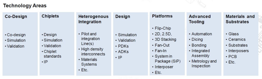
Technologies of interest are shown below:
Yes, I know there are many of you who doubt that we can bring advanced packaging back on shore for economic reasons, but you must admit at least we are focusing on the correct areas.
For all the latest in advanced packaging stay linked to IFTLE………………………


