
The IEDM conference always has a great display of leading-edge technology in the papers, but I always find a great balance of research and development projects, leading-edge, and mainstream technologies at the conference. Over the years, I focused primarily on leading-edge technologies in both mainstream memory and logic, to help determine forecasts, and to help my clients understand what technologies might be coming down the road that they should either prepare for or have a development project already in place. As my focus has changed, I have been looking more in-depth at the integrated packaging space, as 3DICs have emerged rapidly in the world of servers and edge compute. There is a greater need to process greater amounts of data, perform analytics, and artificial intelligence (AI) closer to where the data is collected. New integrated circuits and systems are required to handle the data and reduce the amount of power required to move the data in the system. Below is a small glimpse of some of what was presented at IEDM 2020.
CEA-Leti Provides IEDM 2020 Preface
CEA-Leti opened IEDM 2020 with a virtual seminar that showcased its technology and projects. Titled Efficient and Frugal Solutions for Data Deluge Management, it was kicked off by CEO Emmanuel Sabonnadiere who set the stage for the other CEA-Leti presenters. Sabonnadiere argued that as more of the world moves to edge computing, the industry needs to be energy conscious. He says the electronics industry needs to consider the “Green Equation” as the new paradigm. To do this, new advanced computing that uses less energy is critical, and CEA-Leti has the programs to assist the industry to move into the new paradigm.
The rest of the speakers presented on key programs at CEA-Leti:
- Eleonore Hardy on Addressing Medical and Environmental Challenges with New Sensors
- Eric Mercier on Efficient Wireless solutions for Reducing Power Consumption and Electromagnetic Fields
- Elisa Vianello on Energy Efficient Edge AI Technology
- Maud Vinet on Why Silicon Qbits are the Best Option?
- Marie Sophie Masselot on Smart Solutions for Ubiquitous Security in Data Management
With the focus being IEDM, all of the presentations looked at the role silicon played in the success of these programs. The programs are also focused on key issues facing our industry: Power consumption, quantum computing, sensor management, improved wireless, and security. One thing that stood out to me was, that at a technical conference that is typically dominated by male engineers, 4 of the 5 presenters were women. Françoise will need to make an invite to SemiSisters to all of them.
Back to 3D
IEDM is full of 3D discussions these days. Since the industry moved to copper and greater than three-level metal, the industry has been building skyscrapers in logic silicon; although, memory teams may give me grief about trench capacitors being some of the first 3D work.
The logic transistor continues to be focused on moving from finFET to gate-all-around (GAA). Most of the work at IEDM 202 focused on nanosheets. The papers in Session 2 focused on using Ge, or a SiGe mix to increase the channel mobility. A paper by National Taiwan university used a GeSn material for the channel, which demonstrated excellent channel mobility.
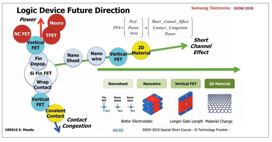
The news leak of TSMC using nanosheets at 2nm and the papers at IEDM suggest that the next transistor technology after FinFETs will be nanosheets and not nanowires. Session Three was one of the sessions on 2D materials, which appear to be moving forward quite nicely. MoS2 appears to be a leading candidate, however, the current process of depositing MoS2, is to deposit the material on sapphire and then pattern transferred to the transistor the WS2 process is fairly similar. Thus, it is unlikely the material transfer process will work in high volume production, so the future challenge will be the deposition of MoS2 or another 2D material on the working transistor. Based upon the papers at IEDM, it looks like it might be a race between the metal sulfides, and carbon in the form of nanotubes and Graphene. Figure 1 outlines the potential path to 2D materials.
Interconnect Challenges
Interconnect continues to be a challenge as there are limits to how low the dielectric constant of the oxide materials can get and still maintain structural and process integrity. Air gaps have emerged as one method that decreases the dielectric constant. As air gaps have appeared in production, I know many dielectric process engineers who blame their gray hairs on developing conformal depositions processes, only to now have air gaps as part of the process flow. SiCN materials appear to be showing promise: although, in paper 20.4 the dielectric constants are still higher than the SiO2 materials. As interconnect dimensions continue to shrink, different combinations of liners are being explored. Co and Ru are leading contenders and, in some cases, maybe in production. While there are definite paths for the transistor to take, the interconnect seems to be running out of options, except for minor improvements in the RC component, or redesign of the interconnect stack. The Design Technology Co-Optimization DTCO session reflected on how to potentially make improvements in memory and logic, including how to potentially improve 2.5 and 3D packaging options for faster computing in the future.
3D Packaging
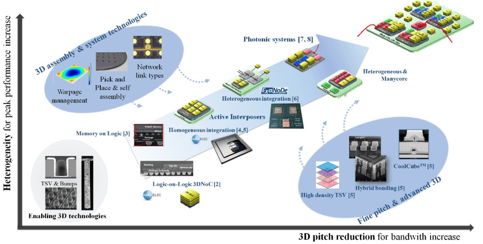
With high-performance computing (HPC) improving 10x every 4 years according to CEA-List, and the planer System-on-Chip (SoC) technology reaching lithography and interconnect technology limits, packaging techniques to continue improving computing performance are emerging. Heterogenous packaging has been a topic at IEDM since chiplets were mentioned by Lisa Su in her keynote in 2017. Global Foundries and ARM, CEA-List, and IMEC made presentations on this topic this year.
Wafer-to-wafer bonding has been a goal since TSVs were introduced back in the early 2000s. IMEC demonstrated bonding both MRAM and SRAM to logic. The key here is to reduce the chip’s power consumption compared to an SoC. Bringing the memory closer to the compute can reduce power consumption considerably and potentially improve latency.

Global Foundries and ARM also presented on hybrid bonding focusing on ARM’s Neoverse system. CEA-List presented an invited talk and discussed how different 3D techniques can be used to develop systems for exascale-level HPC.
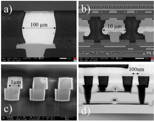
In a conversation with the paper’s presenter, Denis Dutoit of CEA-List, he mentioned that in the 3D world there are multiple tools to create the architecture that will give you the best performance for your product. When using wafer-to-wafer bonding, known good die becomes more of an issue. When creating chiplets, an active interposer is currently a better solution. Attaching memory to logic, hybrid bonding, or finer grain architectures, is the current choice. For grouping logic, analog, and chips of different pitches 10µm or greater, bumping might be the tool of choice. Dutoit commented that ideally, you need to use the right technology for the right architecture. When going from SoC to 3D, need to be able to test and have KGD. Yield needs to be considered, so to a certain extent, it will depend upon the final application. There is a toolbox that you can use, so in any trade, you need to use the right tool for the right application to get the job done.
So, with the existing tools, it will be interesting to see what the industry creates as it moves forward with heterogenous packaging.


