

It’s December, and a busy three weeks of conferences until most of the semiconductor industry takes a short, two-week respite, or at least slow down, while Christmas, New Year’s, and other holidays are celebrated across the globe. Historically, for me the next two weeks have been one of my favorite parts of the year, starting with Semicon Japan, and followed up by the International Electron Device Meeting (IEDM). This year my focus will primarily be on IEDM 2020, but I may sneak in a few SEMICON Japan meetings if my schedule allows.
This year’s IEDM Theme is, Innovative Devices for a Better Future, but as with most semiconductor and packaging conferences, there is a great deal of 3D being built into our future.
3D at IEDM 2020
Typically at IEDM, the big news is advancements in transistor technology. In the past, companies have introduced strain in the transistor, High-k metal gates, FinFETs, and gate-all-around (GAA) technology. IEDM 2020 will be no different. Intel, IBM, IMEC, and National Taiwan University, kick off the technical sessions, with the near future of the transistor, demonstrating nanoribbons, and gate all around (GAA) technologies.
Figure 1
It is projected that TSMC will be bypassing the nanowire technology, and be using nanoribbons at their 2nm technology node. TSMC does not appear to be presenting on GAA technology at IEDM this year which could mean that they are close enough to a solution they don’t want to give away any possible process techniques to help the competition.
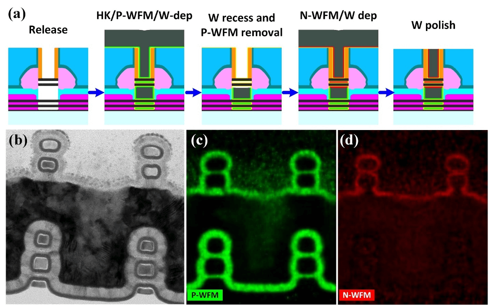
With heterogeneous computing coming of age, Session 15 will present multiple papers on 3D IC technology. ARM and Global foundries were highlighted in the Monday Press conference. With a face to face hybrid wafer bonding process.
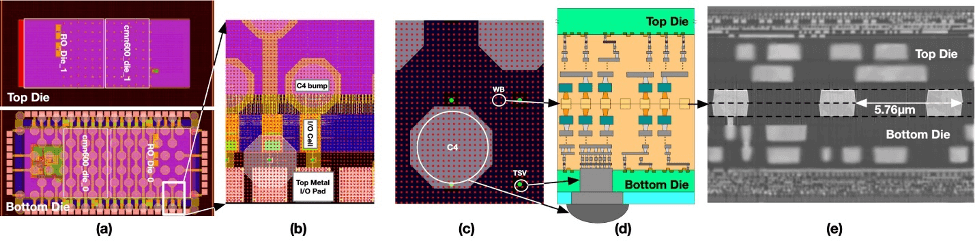
There are five other papers in this session highlighting different techniques that will be used in the future for heterogeneous computing. CEA-Leti, and Imec, will present on heterogenous packaging technology while, QUALCOMM and KAIST, and a joint paper presented by several universities, Tohoku, Hitachi High Technology corporation will discuss monolithic transistor integration.
![[err-ad-fallback-title]](http://www.3dincites.com/wp-content/plugins/a3-lazy-load/assets/images/lazy_placeholder.gif)
Rounding out the 3D discussions will be talks on memory; DRAM, NAND, MRAM integrated into the logic BEOL stack and other emerging memories all of which have unique 3D features.
However, IEDM is more than just 3D structures. In the leading-edge areas, Quantum bits or quantum computing is beginning to move from R&D to reality, as IMEC will discuss during the conference. For me, it is exciting to see 2D materials move both into the transistors, and the interconnect. MoS2 in the transistor, and graphene in the interconnect. Ferroelectric materials continue to advance in memory, and SiC and GaN continue to emerge in the power semiconductor space.
There are 41 sessions with 220 papers. Typically, an attendee might attend 2-3 sessions a day during the live conference, and then read the abstracts for other topics of interest, missing out on the slides and the talk track. With the conference being virtual this year attendees have the opportunity to attend as many sessions as they might wish, and are able to digitally send questions, which can be answered even after the conference closes. This enables them to see a great deal more of the conference virtually than one can do live. This is one of the aspects of virtual conferences I will miss. Hopefully, we will see some form of a hybrid conference in 2021. If you haven’t registered, there is still an opportunity to do so on December 12th


