


It’s been two years since I last visited EV Group headquarters in Schärding, Austria, so I was glad to be able attend EVG Technology Day on February 17, 2016 at the Fremont Marriott, in Fremont CA. It was a good reminder of the company’s many and varied capabilities in processes targeting 3D and MEMS, and I learned lots more about photonics and nano-imprint lithography (NIL).
The first half of the day focused on developments in photonics and heterogeneous integration, and the processes in EVG’s wheelhouse that enables them. It was interesting to see how processes developed for MEMS and 3D have become part of this picture, as they enables photonics integration. Wafer bonding was discussed as a key enabling technology for photonics, as well as discussion about the original 3D integration application for photonics applications – CMOS image sensors with ICs.
The middle session of the day drilled down into nano-imprint lithography (NIL), which involves laying down nanometric scale patterns on substrates. I discovered that I’m not the only woman in the industry to hold a title of royalty. Christine Thanner, the recently crowned “Queen of NIL”, not only explained in detail the difference between hot emboss, UV NIL, and micro-contact printing, but she came bearing gifts for her royal subjects – samples of soft print NIL. Most NIL applications today are related to photonics or photonics principals, including wafer-level optics, various types of lenses, optical gratings, photonics crystals, anti-reflective structures, and biomedical applications with optical detection principals.
The closing session for the day was devoted to 3D and MEMS, and for me, was mostly a refresher course in 3D processes and EV Groups capabilities, with a focus on temporary bond/debond process, as well as improvements in permanent bonding alignment processes, and specifically, Ziptronix DBI process. For a 3D newcomer, it was particularly informative. The highlight of this session was the presentation by Caroline White, AM Fitzgerald and Associates, on the importance of collaboration in developing new MEMS devices.
As this was a customer symposium, the heart of most of the presentations focused on processes and tool capabilities targeting specific customer needs. However, I did come away with some key technology take-aways, the most compelling of which were about heterogeneous integration of photonics technologies.
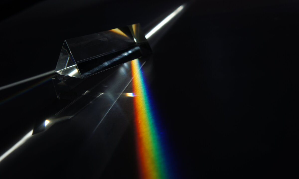
Martin Eibelhuber, business development manager, EVG, defined photonics as the science of light generation, manipulation, and detection. It has a wide range of applications including, image sensors, lasers, LEDS, photovoltaics, optical MEMS, photonic integrated circuits (PICs) biophotonics, optical sensing, and displays.
S.J. Ben Yoo, PhD, professor at UC Davis, talked about photonics as a solution to the “red brick wall” the industry has been facing with regard to scaling. To achieve the necessary performance combined with power efficiency, Yoo says, “electronics alone cannot do it. We have to involve photonics.”
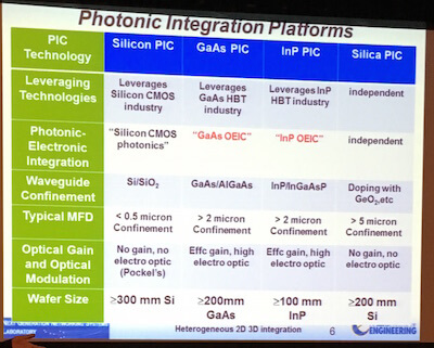
In this case, heterogeneous integration is not just about integrating disparate technologies, but also different materials. Yoo talked about various PIC platforms based on substrate materials, including Si PICs, GaAs PICs, InP PICs, and Silica PICs. Figure 2 provides comparisons of the platforms. Yoo noted these combinations add new challenges for fabrication and design rules.
![[err-ad-fallback-title]](http://www.3dincites.com/wp-content/plugins/a3-lazy-load/assets/images/lazy_placeholder.gif)
Here’s where EVG’s variety of wafer and die transfer capabilities come in handy, particularly when dealing with substrates of various sizes. For example, according to Eibelhuber, EVG offers low-temperature plasma activated bonding processes for low-cost wafer scale integration of 150mm InP to Si direct wafer bonding. As the wafers are different sizes, they take a collective die-to wafer bond approach.
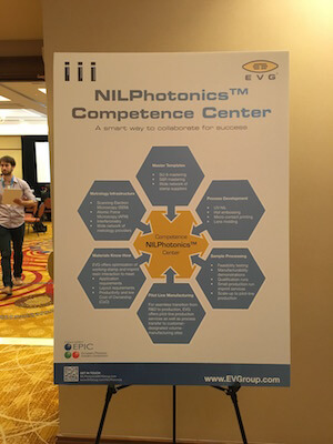 As part of the focus on NIL and photonics, EVG’s Garret Oakes gave an update on the NILPhotonics Competence Center that was established by EVG in 2014 as a “center of excellence that brings the necessary elements for NIL and Photonics integration together in one spot.” The center is the culmination of efforts to source industry partners to bring whole process together. “It’s not easy to get all these elements together in one place,” said Oakes. The entrance barrier for NIL adoption is relatively high. The goal is to help customers minimize risk by having the ability to see what’s behind the demonstration, and understand what tools work best for a given process. The NILPhotonics Competence Center includes dedicated, global process teams, pilot-line production facilities and services at its state-of-the-art cleanrooms at EVG’s headquarters in Austria as well as its subsidiaries in North America and Japan.
The overarching message for the day was about the effectiveness of collaboration. Yoo and White both discussed successful collaborations between UC Davis and EVG, and AM Fitzgerald and Associates, respectively. As with the NILPhotonics Competence Center, the advantage of collaboration is always cost-effective new technology development with a faster time-to-market than would be achieved by going it alone. This was EVG’s first Technology Day for 2016. If you’re in Shanghai on March 15, you can catch the next edition.


