
Latest Posts - Page 9
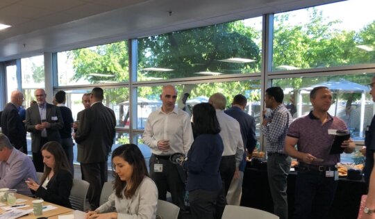
Arizona SEMI Breakfast Forum Focuses on Sensors Enabling a Connected World
Why are sensors not on the same growth trajectory as CMOS? In the face of a shaky global economy, where...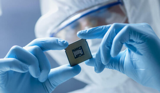
SEMI’s Strategic Materials Conference Calls for Supply Chain Cooperation
The message remains consistent: following Moore’s Law is no longer economical for most IC designs. A major part of the...
SEMICON West 2018: Smart Starts Where?
Well, that was interesting. SEMICON West 2018 just wrapped up, and I’m not quite sure what just happened. This year’s...
Strategic Partnership with ESD Alliance Extends SEMI’s Reach to Semiconductor Design
On Monday, April 16, 2018, SEMI, the industry association representing the global electronics manufacturing supply chain, and the Electronic System...
Packaging, Innovation, and Our Application-Driven World
MEPTEC lunches, now known as the MEPTEC / IMAPS / SEMI Semiconductor Speaker Series Luncheon sponsored by Chip Scale Review,...
Citius, Altius, Fortius: Packaging Topics at SEMICON Korea 2018
Winter 2018, and Korea is at the center of the world in both sports and in electronics. Sports, of course,...
SEMI ISS 2018: AI, IoT, Automotive to Fuel Industry Growth
HALF MOON BAY, Calif. — January 17, 2018 — The SEMI Industry Strategy Symposium ( SEMI ISS) opened yesterday with the...
Notes from SEMI’s ISS 2018, Days 2 and 3
The remaining two days of SEMI’s ISS 2018 dawned foggy and damp, making it a heck of a lot easier...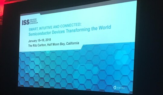
Notes from SEMI’s ISS 2018, Day One
SEMI’s Industry Strategy Symposium (ISS) has been on my conference bucket list for some time, so when I was offered...
New SEMI Japan President to Drive SEMI 2.0 in Japan
SEMI today announced the appointment of Masahiko (Jim) Hamajima as president of SEMI Japan. Reporting to SEMI president and CEO...
Continental Drifts or Tectonic Shifts? Advanced Packaging 2017
That’s great it starts with an earthquake … R.E.M. Boxing Day 2017 ended with an earthquake in Silicon Valley, at...
SEMICON Europa 2017: Connect, Collaborate, Innovate, Grow and Prosper
I remember the day I became Queen of 3D like it was yesterday: It was 2007 and I was attending...
Smart Factories: Is the Semiconductor Industry Practicing What it Preaches?
I’ve often found it somewhat ironic that those responsible for dreaming up and building the technologies that made smart devices,...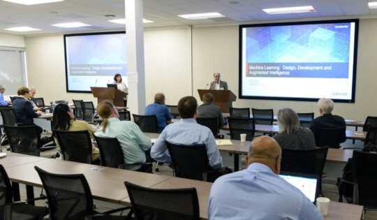
EDPS 2017: NOT the usual Electronic DESIGN Process Symposium
When planning the 24th EDPS, the organizing committee, chaired by Shishpal Rawat, former Intel executive, took a number of bold...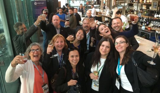
The Brighter Side of SEMICON West 2017
Generally, I avoid reading other journalists’ coverage of events I’ve attended until I’ve had a chance to finish my own...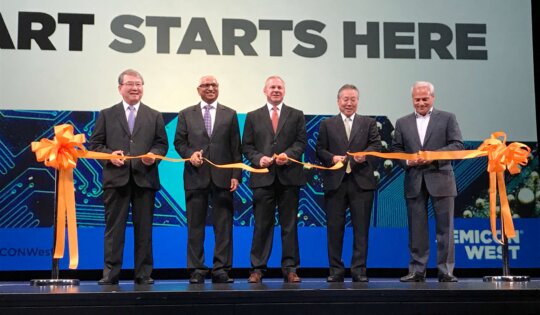
SEMICON West 2017: The Semiconductor Industry at a Young 50
The semiconductor industry is acting quite young for its age. And that’s just not me saying it; over and over...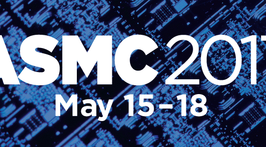
Heterogeneous Integration Makes an End Run Around 7nm Silicon at SEMI ASMC 2017
I like to think that someday soon a perfectly ripe tomato growing on a vine is going to signal its...
Panel Level Packaging: One Size Fits All?
There is an active and robust supply chain currently supporting these wafer sizes in the semiconductor manufacturing industry: 3”; 4”;...