
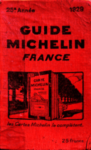
 With nary a farewell glance in the rearview mirror at the terrain successfully covered over the decades during which we followed the ITRS’ Guide Michelin; the new Heterogeneous Integration Roadmap gives us eyes on what comes next. It looks from here-and-now all the way to a horizon that extends, like a straight highway crossing America’s vast Great Plains, a long way out.
Fifteen years out. A long way indeed.
Goodbye, International Technology Roadmap for Semiconductors.
Hello HIR.
You may have read, as I did, that “The Heterogeneous Integration Roadmap (HIR), initiated by the IEEE CPMT Society, and joined with IEEE EDS and Photonics Societies and SEMI, will follow directly the purpose, process, and format of the ITRS Heterogeneous Integration Roadmap … while expanding the vision to address the major changes in the marketplace, and the disruptive changes in technology and the industry.”
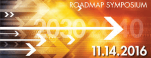
And if you had been present at the recent MEPTEC 2016 Semiconductor Packaging Roadmap Symposium in San Jose, CA, November 14, 2016, as I was, you would have heard Bill Bottoms, Chairman, Third Millennium Test Solutions and Co-chair, Heterogeneous Integration Roadmap, say words to make glad all hearts hearing them: “This is the best time in history to be in the packaging business.”
Heartening words indeed from Dr. Bottoms, particularly because they were in the context of a talk where he reminded us that we have lost CMOS scaling and are, therefore, in “The Chaos Period.” (Tell me about it!)
Per Bill, chaos breeds uncertainty, but it also breeds innovation. (“Chaos,” from the Greek, means “yawning” or “gap”. What forms the bounds of this lacuna was reportedly unclear to the Greeks, but it is not to us: ITRS – Chaos Period – Heterointegration.)
 In the Chaos Period, devices must “do nothing well” as the basic requirement for an Internet of Things (IoT) component deployed in the fog, at the edge, existing on its own power; it is a cryptic description that brings to mind Zen Koans; maybe “When you can do nothing, what can you do?”
It is likely that our present network architectures, when they are loaded with IoT extensions, will experience latency increases, power increases, and cost increases even as consumers clamor for continued decreases in each (cost, power, latency), decreases we have all come to expect in the era of Moore.
This is the best time in history to be in the packaging business.
Regarding latency, what if we had an interconnect technology that is distance agnostic? So asked Professor Lionel Kimerling, MIT, in his talk on “Grand Challenges and Timelines for Electronic – Photonic Integration,” which segued smoothly from Bill Bottoms’ comment that “Photonics to the chip – now that people are building it I’m going to have to change my mind.”
Embedded SiGe-based photodetectors and modulators, photons rather than electrons, the integration of optical interconnection with integrated microelectronic circuit chips, bringing photons closer to the chip.

This is the best time in history to be in the packaging business.
The jury is still out on whether to call them Chiplets, or Dielets, but I’m not going to let that stop me from thinking, as Subu Iyer (UCLA), Dan Green (DARPA), and David McCann (GLOBALFOUNDRIES) also do, that heterogeneously integrating very small devices using some kind of silicon-based (or glass-based) interconnect fabric is a pretty terrific idea from a cost perspective, and also from a performance one.
Small die = better die yield = lower cost die; heterointegration = performance advantages when you combine just enough silicon transistors from one chiplet with just enough compound semiconductor transistors from one dielet.
“Louie, I think this is the beginning of a beautiful friendship.”
Many thanks to MEPTEC for organizing the Roadmap Symposium, to Association Sponsors CPMT, EDS, ESDA, and SEMI, and to the wonderful speakers who, with passion and also with a good bit of humor, made the day the success it was.
Whether it is a matter of our technology moving on, or disruptions in the personal sphere, change in all its forms, we must embrace the dislocations, create and follow a new map, and not never look back, but be mindful of mostly looking forward.
According to Professor Andrew Kahng, UCSD, in a voice holding great conviction, “Heterogeneous integration is where the future lies.”
This is the best time in history to be in the packaging business.
Ordo ab chao. Out of Chaos comes order.
From Santa Clara, CA, Happy Thanksgiving, and thanks for reading. ~PFW


Optimism not burdened with theoretical understanding of the challenges / cost of heterogeneous integration ! Which of these “experts” and starry eyed “academics” lately turned boosters of dielets would like to explain why planar 2.5 d or TSV based stacks ( e,g HBM ) cost quite so much, a cost differential for new Packaging technology about 2x that of previous major innovations like Flip Chip, w/o the corresponding improvement in performance ? Go check Fury or Pascal benchmarks. And why is Samsung fast back pedaling to HBM 3 ?
Dev,
Thank you for your comments. Point well taken. Cost is King, always, but when it makes sense (CMOS Image Sensors, for example) we do see TSV-based stacks in consumer products, even with relatively low ASPs. And when performance is King we see TSV-based stacks and 2.5D structures in examples like the latest NVIDIA GPUs. AMD products too.
With so many engines pulling the heterogeneous integration train, including the recent enthusiasm for dielets, I won’t be surprised to see some kind of rapid take-off, as we did with FOWLP, for which I was initially a skeptic.
Hi Paul :
Hope you are still checking this Board.
You are absolutely right of course when it comes to end users with deep pockets like Google for who getting going with their Inference Engines ASAP is far more important than saving from their billion dollar R&D budget a mere few million bucks for hardware for which they would have to wait for Foundries & OSATs to develop technologies cheaper than current stacks interconnected by TSVs or 2.5 d interposers w/ Dual Damascene line densities. This is also true even for Googles’ smaller competitors in the hot field of Inference Engines / Machine Learning that is now flooded w/ VC money. These latter will have no second thoughts about lining up for nVidia’s expensive Pascal GPUs that pretend to be array processors and use expensive HBM2 and 2.5d w/ DD. But when it comes to the somewhat cost sensitive Graphics / Game modules ( not all Gamers are raving lunatics after all ) it is instructive to look up AMDs latest roadmap – for the foreseeable future last year’s Fury w/ 4 GB of HBM 1 on DD 2.5d is to remain an one off experiment ! And Intel has already shown that for their multi core CPU that is dominant in the Server world, one can integrate HMC to organic flip chip substrates and still come out ahead Bandwidth wise – so much so as to make their modules a top contender for Supercomputers to do serious work ( design more potent Nukes ). The same goes for the much larger volume Network controllers. Only for I/O intensive processor designs ( like FPGAs where 5 years ago the first 2.5d had been used to cover up low yield of very large dies at an immature node – at that time 28 nm at TSMC ) where high line density is critical for escape, it is not really necessary to make the whole interposer out of DD Si but selectively embed high density ( L/S 2 um ) pieces of Si on regular SAP organic substrates ( L/S 12 um ). Based on past history, even as we speak TSMC is probably furiously trying to replicate the much cheaper / elegant Intel approach ( EMIB ) that requires a little bit more of process technology to lower the cost of 2.5 d but just as they had done with their 2.5 d or FO WLPs, TSMC will probably come out with an entirely new name for it to impress their naïve customers and hangers on in the now Fabless Si Valley.
But not so suppliers about mestacked mewhen it comes to like Google e