

On Monday, April 16, 2018, SEMI, the industry association representing the global electronics manufacturing supply chain, and the Electronic System Design (ESD) Alliance, representing the design community, announced a strategic partnership. On Tuesday I had a very informative conference call with Bettina Weiss, VP Business Development at SEMI and Bob Smith, Executive Director, the ESD Alliance to discuss the strategic partnership they are spearheading.
The ESD Alliance joins SEMI as a Strategic Association Partner; the latest in a string of previously independent organizations that have been absorbed under the SEMI umbrella including the FlexTech Alliance, the MEMS and Sensors Industry Group and the Fab Owners Association. Like the others, the ESD Alliance will continue its traditional mission, representing the interest of the semiconductor design ecosystem. It will retain its own governance and drive its own initiatives and direction. Weiss and Smith explained that the partnership with SEMI gives the ESD Alliance and its members access to SEMI’s worldwide resources, programs like workforce development, economic and legislative initiatives and, of course, better access to SEMI’s membership. SEMI and its 2000 members benefit from this partnership because SEMI will extend its focus beyond the manufacturing supply chain, into the semiconductor design space. This will lead to anticipating and preventing likely manufacturing challenges already during the design steps, resulting in faster production ramp-ups and lower unit cost.
Enough about the official announcement, which was covered widely by the trade press. To highlight the significance of this agreement and the value it brings to both organizations’ members, allow me to expand on some of the topics we discussed with my own thoughts: I believe this alliance will allow for better strategic planning and will bring structure to the traditionally tactical and project-based cooperation between semiconductor design and manufacturing supply chain members.
During my first twenty years in this industry, I enjoyed the well-coordinated design and manufacturing efforts within IDMs, because we all had the same corporate objectives and one management’s directives to follow.
More than 20 years ago, the transition to the fabless IC vendors and wafer foundries business model divided design and silicon manufacturing steps into independent companies with their own objectives, schedules, and strategies. The major wafer foundries reacted well to this new challenge by structuring the cooperation between suddenly independent entities. They developed process design kits (PDKs) and, together with EDA partners, reference flows to enable and accelerate the fabless IC vendors’ silicon planning, design and verification steps.
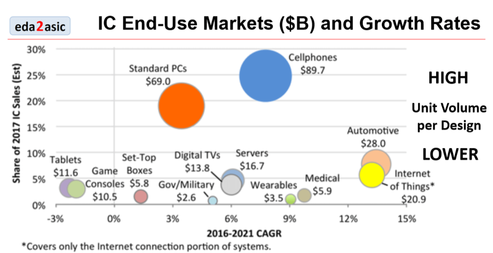
As usual, customers are demanding smarter and more capable electronic products with every new generation. This leads our industry to develop more system-level solutions that integrate heterogeneous functions, in addition to shrinking logic transistors’ feature sizes. To meet, in a timely manner, the economic and technical requirements that automotive, computing, networking and many other semiconductor applications impose, both the supply chains for design and manufacturing need to work together more closely than previously was necessary. Also, as a market analysis (Figure 1, below) shows, the traditional growth drivers of the semiconductor industry, high volume PCs, and cellphone designs can no longer drive revenue and profit growths, at previous rates.
Automotive, IoT, medical and other diverse application will drive semiconductor industry growth in future. Their typically lower volumes per design project will demand increasing engineering productivity to lower development cost. Better cooperation between all contributors in the design AND manufacturing supply chain will make this transition successful. Also, new technologies, like multi-die ICs and modules (2.5D, 3D, WLP, SiP,…) and flexible hybrid electronics (FHE) will enable true system-level integration and increase the value of the solutions our industry provides.
In system-level solutions, IC packages, PCBs, connectors and other mechanical components play a much more important role in creating value than in single-die SoC designs. They’ll also create many new challenges, encouraging even more strategically planned and well-structured cooperation between all design and manufacturing experts.

Last, but certainly not least, workforce development becomes a very critical component for a smooth transition to providing higher value solutions, comprising many more heterogeneous and multi-physics building blocks than SoCs. The increasing number of industry conferences, higher demand for on-site training as well as more design and manufacturing services, are early indications of our industry’s response to these new challenges.
On a more personal note, just a few examples of how difficult it can be for a large company to make a strategic change and the consequences I have seen:
- Encouraging VLSI Technology to work with TSMC to lower silicon cost failed and lead to VLSI’s demise.
- Bringing Synopsys and TSMC together was very difficult, but significantly contributed to both companies’ success.
- Introducing more EDA capabilities to major IC Assembly & Test houses, took a long time, but now shows real promise.
- More and more industry conferences include both design and manufacturing topics in their agendas (A) as well as many design and manufacturing experts, demonstrate interest and commitment to learn about each other’s capabilities and challenges and discuss how to cooperate on projects.
Bottom line: The strategic partnership between SEMI and the ESD Alliance will enable member companies to adapt to new market requirements faster and at lower transition cost. It will help experts on both sides to replace costly and high-stress tactical, project-based cooperation with well-structured and industry-wide agreed-upon best practices even, where applicable, standards.
Please join me at the following design AND manufacturing focused conferences: ~ Herb


