
That’s great it starts with an earthquake …
R.E.M.
Boxing Day 2017 ended with an earthquake in Silicon Valley, at 10:32 pm, a magnitude 3.9 temblor near Alum Rock I thought could have been my neighbor dropping something heavy in the apartment upstairs, except that nobody lifts and drops anything that heavy, for that long, in the building where I live.
 No reports of damage, but the shaking came as a good wake-up call to have those basic earthquake kit supplies (water, flashlight, light food, warm clothes, etc.) somewhere within easy reach, and to have a family plan for how and where to meet when The Big One comes.
It’s also got me to thinking whether or not 2017 was witness to a tectonic shift in semiconductor device packaging.
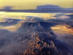
According to NOAA, “Our planet looks very different from the way it did 250 million years ago when there was only one continent, called Pangaea, and one ocean, called Panthalassa.”
Today, the surface of our planet is composed of tectonic plates, which “… move toward and away from each other at an average rate of about 0.6 inches a year. … At the ‘seams’ where tectonic plates come in contact, the crustal rocks may grind violently against each other, causing earthquakes and volcano eruptions.”
Wasn’t all semiconductor device packaging at one time all the same kind of packaging? As I remember from my early Intel days it was only ceramic dual in-line packages (CERDIPs) that we saw, whether for the microprocessors (8088), microcontrollers (8048), or erasable programmable read-only memory (EPROMs) (2732) that we made.
One continent, called Pangaea, and one ocean, called Panthalassa.
(BTW, “The relatively fast movement of the tectonic plates under California explains the frequent earthquakes that occur there.” We move fast and break things.)
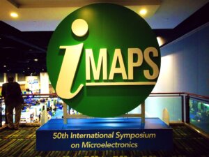 My semiconductor packaging conferences in 2017 were back-end loaded, meaning IMAPS and IWLPC in October 2017, MEPTEC in late November, EPTC 2017 in early December, and then SEMICON Japan in the middle of the month.
I gave talks (on physical vapor deposition (PVD) for fan-out packaging, both wafer level, and panel level) in San Jose, Singapore, and Tokyo, and I sat in on the meetings SEMI now has up and running for the new fan-out panel level packaging applications standardization effort SEMI launched last month.
And, after listening to the myriad of distinguished talks from the many learned speakers at those assorted conferences, I like sitting here at year-end, imagining each of the advanced packaging technologies — be they flip-chip, or fan-in, or fan-out — as moving continents, bumping up against each other, with the occasional earthquake or spouting volcano as the visible result. (Right, Françoise?)

Those advanced packaging continents and plates aren’t just bumping up against themselves either – advanced packaging is bumping up against the big continent itself, Gondwana, the Moore’s Law supercontinent, and the resulting energy transfer is the heat advanced packaging feels as one of the “More than Moore” paths the semiconductor industry is counting on to ensure our continued technological progress and our continued commercial success.
Merriam-Webster defines the adjective “tectonic” as “having a strong and widespread impact.”
There are large-scale processes (panel level packaging!) underway today that are surely going to punctuate our present equilibrium, just as the shift to plastic packages punctuated the equilibrium in my Intel fab all those decades ago.
I’d say 2017 was a year with continued movement of the tectonic plates we ride in semiconductor device packaging, a year of (productive) continental drift, even though we didn’t quite achieve a tectonic shift, yet, in our day-to-day.
And I will also say that a true tectonic shift is coming, and soon, as a result of the kinds of system-in-package (SiP) heterogeneous integration schemes that fan-out packaging accommodates so well.
 I’ll be seeing you at SEMICON Korea 2018 if you go, and at DPC 2018 too.
Until then, dear readers, I wish you the Happiest of Happy New Years, one filled with Peace and Prosperity … and loads and loads of advanced packaging.
From Santa Clara, CA, thanks for reading. ~PFW


