
Winter 2018, and Korea is at the center of the world in both sports and in electronics.
Sports, of course, because of PyeongChang, host city for the 23rd Olympic Winter Games, with participants ranging from Eritrea to Tonga, along with the usual cold-weather-country (Norway, Canada, Sweden, etc.) players who showed up for the Games.
And electronics, of course, specifically semiconductor device fabrication and packaging, because of SEMICON Korea 2018, with participants ranging from Amkor to SK Hynix to Samsung, along with the usual members of the semiconductor manufacturing supply chain, both international and home market, who showed up for the Show.
As SEMI has it, “Semiconductor industry sales in 2017 topped $400 billion for the first time, up 22 percent year-over-year, ‘a feat made possible thanks to the great contributions of Korean companies,’ said Ajit Manocha, president and CEO of SEMI, at last month’s SEMICON Korea. Manocha went on to note that he expects Korea to continue heavy semiconductor spending in 2018 – with Samsung and SK Hynix accounting for as much as a staggering ‘40 percent of semiconductor industry investments.’”
And about the show itself, per SEMI, “SEMICON Korea – at COEX, Seoul from January 31 through February 2 [2018] – also grew, drawing more than 50,000 visitors to the premier event for the electronics manufacturing supply chain, up 20 percent from last year. The sold-out exhibition featured 1,913 booths, the most in the event’s history, and 436 participating companies spanning the entire semiconductor industry supply chain including the equipment and materials, component, design, software and facility sectors.”
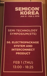
I’ve been treating recent SEMICONs as much for their benefits as focused technical conferences as I have been treating them as big trade shows. (Araby! Pace, James Joyce.) SEMICON Korea 2018 was no different, except that part of the focused technical conference this time was me, presenting my paper on ion beam pre-clean for fan-out packaging, at the Electropackage System and Interconnect Product technical session SEMI organized for the afternoon of 01 February 2018, and from which I send this report.
 I was in excellent company! The other presenters represented local interests (Amkor, SK Hynix, KAIST, nepes, Samsung), regional biggies (ASE, STATS ChipPAC, now known as JCET), the foundry world (GLOBALFOUNDRIES), the next-big-thing (NVIDIA), and the ones who watch and draw conclusions (Yole Developpement).
The standing-room-only crowd was treated to these insights and observations from the afternoon’s distinguished speakers:
STATS ChipPAC aka JCET told us about the rosy future growth forecast for automotive electronics in general (15% CAGR through 2025) and for Advanced Driver Assistance Systems (ADAS) content specifically (30% CAGR through 2025, reaching a market value of over $5B in semiconductor content). Fan-Out Packaging (FOWLP, in the form of eWLB) is the most attractive packaging solution for the mmWave Radar systems upon which current and future ADAS sensors are based, 77 GHz (or higher frequencies) Radar being the best all-around sensing technology for autonomous vehicle “vision” and eWLB fan-out being the best packaging technology, from an electrical performance standpoint, for these high-frequency applications.
I had never considered Cu pillars as part of the UBM until now, but I am now reset in my thinking, thanks to the fascinating talk on “Bump Electromigration Reliability of Fine Pitch Interconnects” by Dr. Seung-Hyun Chae, SK Hynix. Dr. Chae presented compelling data to show how the “ever-increasing demand for high performance and small form factor in microelectronics packaging raises concerns on electromigration (EM) reliability of solder joints in advanced packages.” Many excellent images and figures in this talk of how the “EM performances of fine-scale solder interconnects used in advanced packaging technology, including stacked-die packages with through-silicon vias (TSVs) and flip chip packages” are a function of the metallurgy itself (morphology, presence of intermetallic compounds, IMCs), and of the electrical and thermal stresses these interconnects must endure, without failing under those stresses, particularly for the stringent reliability expectations of the automotive market.

Chip first, or chip last? There’s still a healthy debate on the subject, said YoungRae Kim, Amkor, in his talk on “Evolving in Fan-Out Technology for Next Generation Applications,” covering an evolving world where multi-chip packaging is becoming increasingly important.
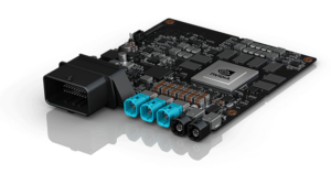 And in his invited talk, Junghoon Cha, NVIDIA, posits that we basically stand at the threshold of a new computing era, the era of AI, the next stepping stone in the progression that has already taken us from the PC to the Smartphone to the wonders of the Cloud. GPU-type architectures have literally sent us off the chart (or at least off the business-as-usual CPU computing performance chart), enabling the world of sensor-laden autonomous vehicles running on supercomputer data centers the size of a license plate, fitted in your vehicle’s trunk (or its boot, if you’re British).
Thin-film flexible electronics are another stone upon which we will step as we make progress to the future, particularly progress on cost, flexible substrates being potentially cheaper than single crystal silicon ones, and progress on use cases, flexible electronics being more compatible with the complex motions of complex human motion – think biomedical, or athletic performance sensors embedded in a speed skater’s suit, or wrapped around a knee or elbow as the joint heals after injury. Those flexible electronics better be mechanically reliable – after all, they are going to bend and stretch and reach for the stars, as Professor Taek-Soo Kim, KAIST, reminded us in his comprehensive talk on just how it is flexible electronic devices fail. Best to understand the fundamental material properties in order to enhance the mechanical properties of these devices, and best to use that understanding to properly design and optimize flexible device structures.
Semiconductor device packaging needs to serve the 4th Industry Revolution (comprising AI, robots, autonomous vehicles) just as well as packaging has served the industry revolutions preceding, and redistribution layer (RDL) technology, says Dr. Se-Ho You, from Samsung, is going to be the workhorse technology. RDLs as used in SiP technology have advantages both in thermal performance and in bandwidth enablement, while RDLs as used in interposer-based systems have productivity and memory density advantages over what came before. Samsung interposer technology with RDL, and Samsung SiP technology with RDL: it’s ready for NVDIA. Dr. You: “[NVIDIA] Please come to Samsung!” (And the audience chuckles in appreciation.)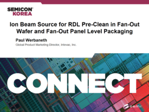
That’s it for Part 1 of my blog; I will end it here by saying my SEMICON Korea 2018 presentation, on “Ion Beam Source for RDL Pre-Clean in Fan-Out Wafer and Fan-Out Panel Level Packaging,” is available to you directly, should you please just ask.
From Santa Clara, CA, thanks for reading. ~PFW