
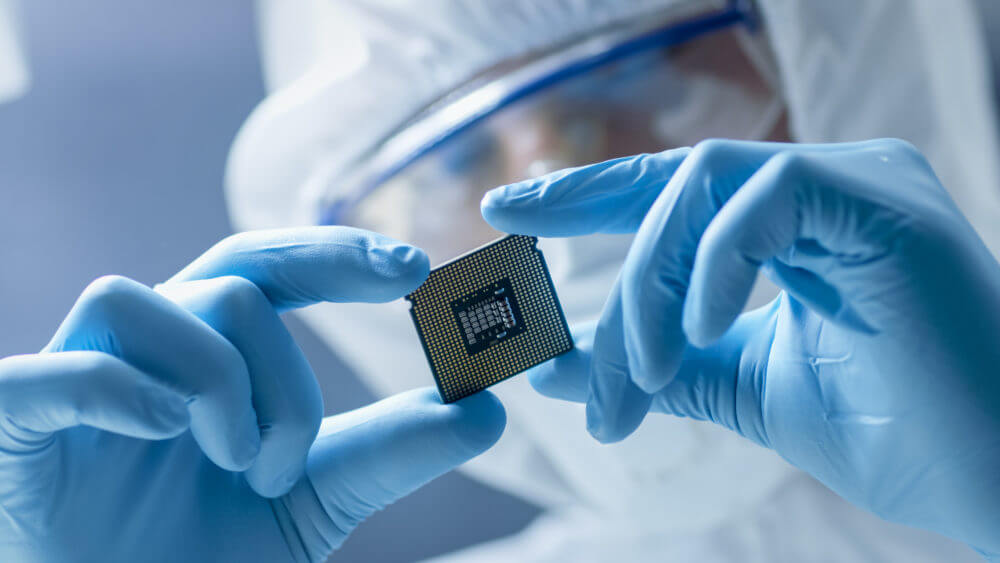
The message remains consistent: following Moore’s Law is no longer economical for most IC designs. A major part of the IC value creation is moving from the die to the IC package. Now advanced packaging technologies and materials enable combining multiple dies with heterogeneous functions as well as high-quality passives into one package.
This integration increases performance, while significantly reducing power dissipation and form factor. However, it imposes a range of new challenges on packaging materials, equipment as well as design, manufacturing and test flows.
To execute timely and cost-effectively, it also demands clear hand-off points, new business models as well as sharing of responsibilities and rewards across all contributing members of the supply chain. This was the focus of SEMI’s well-attended Strategic Materials Conference (SMC 2018), which took place Sept. 23-24 in San Jose.
The future is qubits
The first keynoter, John Martinis, a research scientist at Google and UCSB, took a big step into the future on Tuesday morning. He presented how Qubits will change the current computing paradigm and emphasized that, in addition to the number of Qubits, their quality is very important for high-performance computing (Figure 2).
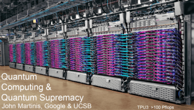
While Martinis did not elaborate on specific materials requirements, the high speeds and operating temperatures below 21o Kelvin he mentioned, tell me that today’s dielectrics and interconnects may be challenged in a quantum computing system. More technical depth about quantum computing is in a brief article by Julian Kelly, another AI Labs research scientist. He explains how the Bristlecone quantum processor works and what it means for Google’s Artificial Intelligence (AI) plans.
The state of solid-state
The second keynoter, Richard New, VP of research at Western Digital (WD), started by reminding the audience that WD acquired Sandisk in May 2016 and with it joined Toshiba 3D Flash developments. New looked back at WD’s hard disk innovations and explained shingled magnetic recording and the heat-assisted write processing. Looking at the solid-state memories, he explained the many processing challenges, as 3D NAND vendors are targeting 192 layers and more.
Memory market puts on the brakes
Risto Puhakka, VLSI Research, talked about market trends and economics. He confirmed that a decline in memory prices will reduce the current revenue growth rate of our industry in 2019 but was optimistic about the longer-term revenue growth. He sees the traditional growth drivers, like PCs, tablets andsmart phones declining, while the server business continues to grow nicely. Because the rapid conversion from 2D NAND to 3D NAND will be completed around 2020, he expects that the currently high CapEx spending by Micron, Samsung and SK Hynix is likely to decline. He warned that China’s actions and reactions in context with the ongoing trade tensions can have a major impact on our industry.
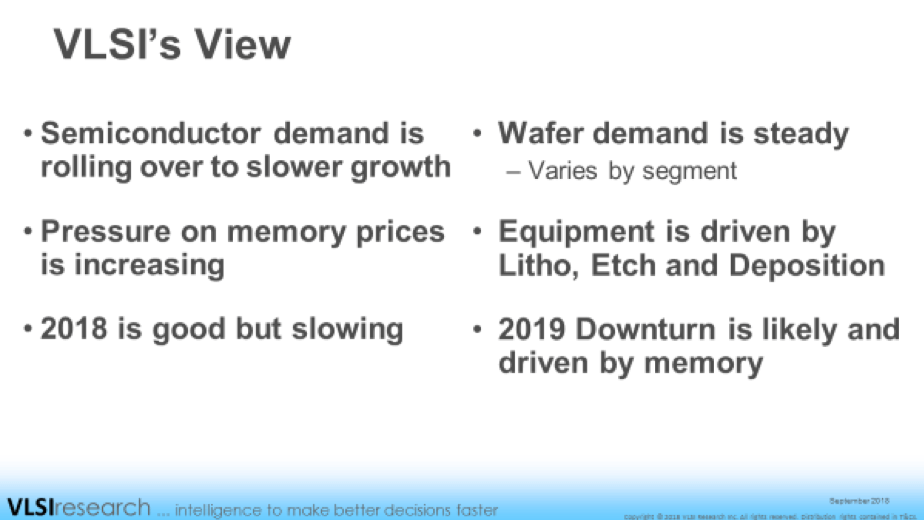
The next market expert, John Pitzer from Credit Suisse, outlined a high-level perspective of our industry. He projected 6-7% CAGR, leading to $ 500B TAM by 2020 and $ 750B by 2025. He also mentioned the possibility of both short as well as long-term dislocations, caused by China.
Scaling further is a material issue
Regina Freed, patterning director at AMAT, stated that the slowing of scaling is not because of resolution and lithography challenges, but is caused by insufficient materials engineering. In addition to new materials, she pushed for local process engineering optimization, co-optimization of materials and self-alignment to be deployed.
Packaging impact on materials
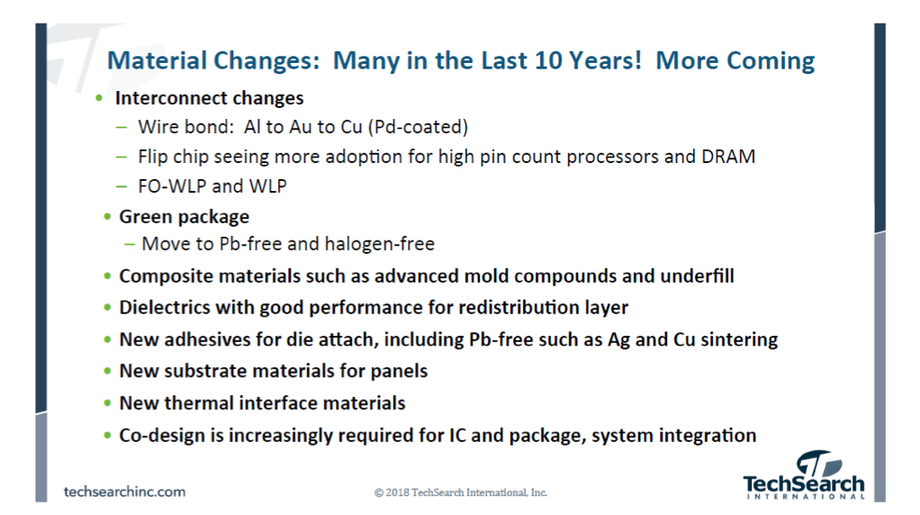
Jan Vardaman, founder and president of TechSearch International, addressed major trends in IC packaging, as outlined in slide 3, and explained how these changes impact materials and the entire supply chain. Please note the last point on her slide, highlighting the need for die-package-board co-design and EDA vendor support!!!
Spotlight on system-level integration
Rozalia Beica, from DowDupont, chaired a session that focused on system-level considerations and heterogeneous integration. Speakers from JCET, Atotech and Henkel outlined their companies’ capabilities to serve specific market needs for integration and highly reliable components and materials.

3MTS’ Bill Bottoms outlined why the ITRS efforts had to be replaced by the Heterogeneous Integration Roadmap (HIR). He showed how many disciplines, from planning and design to materials, equipment, manufacturing, test, and QA need to be addressed and agreed upon, to give our industry comprehensive development guidelines towards system-level integration.
In his Wednesday morning keynote, Rick Hammond, CMO, DowDupont, explained how the company’s broad materials portfolio serves a wide range of applications and emphasized that the semiconductor industry can no longer impress the customers with smaller and smaller feature sizes but needs to provide economical and reliable solutions for their specific and unique system-level requirements.
A word on automotive electronics
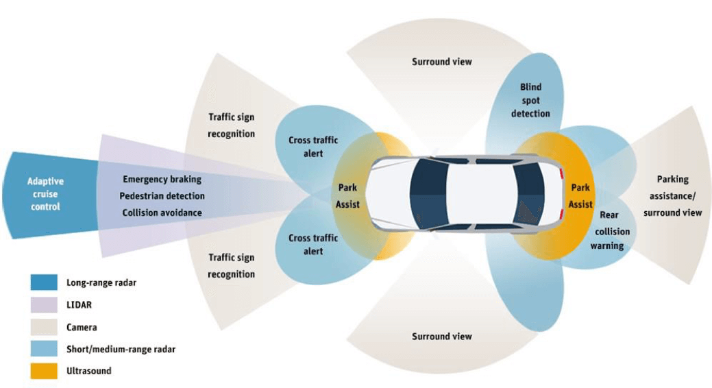
The second keynoter, Ritesh Tyagi, head of Infineon’s automotive innovation center, focused his message on solutions for this high-growth segment. Slide 4 below shows that many sensors, utilizing different technologies, are needed to introduce smart cars and enable autonomous driving. Tyagi explained how accurate but costly LIDAR is and emphasized that only very cost-effective solutions can win in this market (Figure 5).
Collaboration is needed
In the session, titled “Supply Chain Evolution”, Paul Burlingame, CEO at Air Liquid and Kurt Carlsen, a materials consultant, highlighted the need for better cooperation across the entire supply chain. They also emphasized the importance of strategic supplier management, risk and reward sharing, defining IP rights, hand-off points and detailing individual responsibilities.
In the following panel discussion, representatives from a customer (Intel), a design service (Broadpak), a materials company (DowDupont) and a blank wafer supplier (Siltronic) answered questions from Kurt Carlsen, the moderator, and the audience.
Both the comments from the experts on stage as well as questions from the audience clearly showed that everybody is interested and motivated to contribute to the growth of our industry, realizes that the challenges ahead cannot be solved with individual sprints, but will require company buy-ins to arrange knowledgeable and well-coordinated “long-distance runners” to cooperate in the relay race in front of us.
Summary
Like in many previous conferences, all experts I met at SMC 2018, are very knowledgeable in their fields. However, many of their companies have not (yet) decided to join the relay race in front of us. Allow me to encourage more sharing of development responsibilities to reduce the time to profit – just like the fabless IC vendors and wafer foundries cooperation does today. In addition, I want to encourage EDA vendors to join the development of design kits and reference flows to increase engineering productivity across the supply chain. Thank you! … ~Herb


