Challenges to 3DHI and chiplets remain, but new advanced packaging foundry solutions are stacking up
The industry consensus is that the path to extending Moore’s Law lies in heterogeneous integration (HI) and chiplet architectures. Why, then, are we still waiting for the full adoption of HI, 3DHI, and chiplets? The fact is that some significant technology and supply chain hurdles remain.
First, there are design challenges specific to HI architecture. Can the design avoid excessive heat buildup? Do the elements share an adequate interconnect protocol? Can the final device be tested effectively? Few design teams can address these challenges and turn out a successful product.
Second, HI-enabling processes are delicate and demanding. Technicians must deal deftly with wafer bow, CTE mismatch, delamination, etc. The right equipment is not enough; success takes considerable skill and know-how.
Third, HI advanced packaging is a multi-step process. Subcomponents can be manufactured at different fabs, assembled at another facility, and perhaps packaged and tested in yet another. This enables extraordinary flexibility, but it demands close collaboration among all parties. In a supply chain where manufacturers are loath to expose trade secrets to one another, this is difficult to achieve.
A select few companies have mastered the complexities of HI design, manufacturing, assembly, and test. Their 3DHI and chiplet-based products use the best, most advanced processes in the industry. They have built crucial relationships, created new supply chains, and assembled highly skilled teams. They now produce best-in-class operational HI devices.
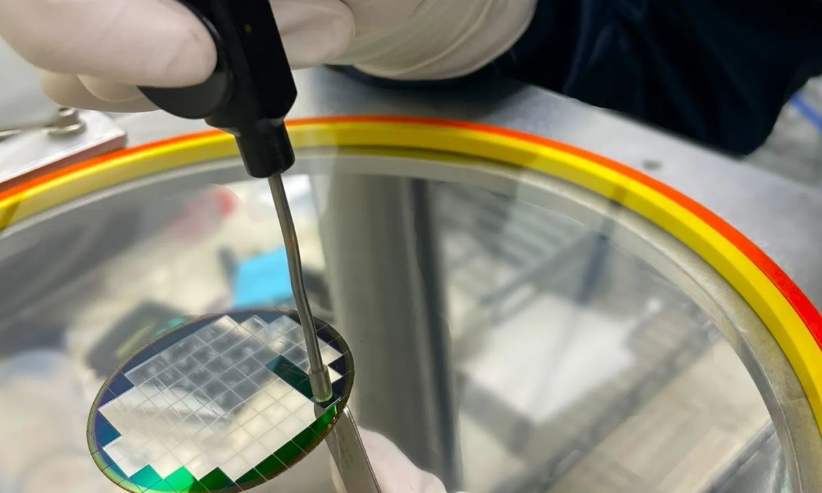
NHanced Semiconductors is one of these companies. We have successfully commercialized the manufacturing of HI, 3DHI, and chiplet devices by applying decades of process development know-how and experience. We employ technologies like hybrid bonding, silicon or glass interposers, chip stacking, and micro-transfer printing to deliver advanced HI devices in volume.
An important part of our business model is that we do not build our own transistors. We start with dies and chiplets from traditional foundries and apply specialized processes to create HI assemblies. We don’t compete with the transistor foundries; thus we avoid the “trade secret” issue.
Another plus: non-transistor processes can be practiced cost-effectively at lower volumes. This flexibility lets us build tailored devices, not just mass-produced commodities. 3D ICs already extend Moore’s Law; our approach adds affordable customization to the menu.
We built on these advantages to create the world’s first purpose-built advanced packaging foundry. We call our new business model “Foundry 2.0™” – and we believe it has the potential to change the industry.
Foundry 2.0 can create system-level solutions that minimize costs and risks while delivering superior performance and faster cycle times. Foundry 2.0™ can reduce development costs for leading-edge chips by up to three orders of magnitude.
We believe the future lies in this new manufacturing model. Leading-edge high-volume foundries will continue building dies and chiplets while nimble Foundry 2.0™ fabs craft those components into sophisticated, highly differentiated HI products.
Bottom line: Foundry 2.0™ is the future. We are proud to be the only US foundry currently supporting this ground-breaking new model.